SNLS289D April 2008 – September 2015 LMH1982
PRODUCTION DATA.
- 1 Features
- 2 Applications
- 3 Description
- 4 Revision History
- 5 Pin Configuration and Functions
- 6 Specifications
-
7 Detailed Description
- 7.1 Overview
- 7.2 Functional Block Diagram
- 7.3 Feature Description
- 7.4 Device Functional Modes
- 7.5 Programming
- 7.6
Register Maps
- 7.6.1
I2C Interface Control Register Definitions
- 7.6.1.1 Genlock and Input Reference Control Registers
- 7.6.1.2 Genlock Status And Lock Control Register
- 7.6.1.3 Input Control Register
- 7.6.1.4 PLL 1 Divider Register
- 7.6.1.5 PLL 4 Charge Pump Current Control Register
- 7.6.1.6 Output Clock and TOF Control Register
- 7.6.1.7 TOF Configuration Registers
- 7.6.1.8 PLL 1, 2, 3 Charge Pump Current Control Registers
- 7.6.1.9 Reserved Registers
- 7.6.1
I2C Interface Control Register Definitions
-
8 Application and Implementation
- 8.1
Application Information
- 8.1.1 148.35 MHz PLL Initialization Sequence
- 8.1.2 Enabling Genlock Mode
- 8.1.3 Output Disturbance While Output Alignment Mode Enabled
- 8.1.4 Evaluating the LMH1982
- 8.1.5 Input Reference
- 8.1.6 Output Clocks and TOF
- 8.1.7 Reference And Pll Lock Status
- 8.1.8 Loop Response
- 8.2 Typical Applications
- 8.1
Application Information
- 9 Power Supply Recommendations
- 10Layout
- 11Device and Documentation Support
- 12Mechanical, Packaging, and Orderable Information
Package Options
Mechanical Data (Package|Pins)
- RTV|32
Thermal pad, mechanical data (Package|Pins)
- RTV|32
Orderable Information
6 Specifications
6.1 Absolute Maximum Ratings
over operating free-air temperature range (unless otherwise noted)(1)(2)| MIN | MAX | UNIT | ||
|---|---|---|---|---|
| Supply Voltage, VDD | 3.6 | V | ||
| Supply Voltage, DVDD | 2.75 | V | ||
| Input Voltage (any input) | −0.3 | VDD +0.3 | V | |
| Lead Temperature (Soldering 10 sec.) | 300 | °C | ||
| Junction Temperature, TJMAX | 150 | °C | ||
| Storage Temperature | −65 | 150 | °C | |
(1) Stresses beyond those listed under Absolute Maximum Ratings may cause permanent damage to the device. These are stress ratings only, which do not imply functional operation of the device at these or any other conditions beyond those indicated under Recommended Operating Conditions. Exposure to absolute-maximum-rated conditions for extended periods may affect device reliability.
(2) If Military/Aerospace specified devices are required, please contact the Texas Instruments Sales Office/ Distributors for availability and specifications.
6.2 ESD Ratings
| VALUE | UNIT | |||
|---|---|---|---|---|
| V(ESD) | Electrostatic discharge | Human body model (HBM), per ANSI/ESDA/JEDEC JS-001(1) | ±2000 | V |
| Machine Model | ±200 | |||
(1) JEDEC document JEP155 states that 500-V HBM allows safe manufacturing with a standard ESD control process.
6.3 Recommended Operating Conditions
over operating free-air temperature range (unless otherwise noted)| MIN | MAX | UNIT | ||
|---|---|---|---|---|
| VDD | 3.135 | 3.465 | V | |
| DVDD | 2.375 | 2.625 | V | |
| Input Voltage | 0 | VDD | V | |
| Temperature, TA | 0 | 70 | °C | |
6.4 Thermal Information
| THERMAL METRIC(1) | LMH1982 | UNIT | |
|---|---|---|---|
| RTV (WQFN) | |||
| 32 PINS | |||
| RθJA | Junction-to-ambient thermal resistance | 33 | °C/W |
(1) For more information about traditional and new thermal metrics, see the Semiconductor and IC Package Thermal Metrics application report, SPRA953.
6.5 Electrical Characteristics
Unless otherwise specified, all limits are specified for TA = 25°C, VDD = 3.3 V, DVDD = 2.5 V.| PARAMETER | TEST CONDITIONS | MIN(2) | TYP(1) | MAX(2) | UNIT | ||
|---|---|---|---|---|---|---|---|
| IVDD | VDD Supply Current | Default register settings, no input reference, 27-MHz VCXO and loop filter connected, 100-Ω differential load on SD_CLK and HD_CLK outputs; no load on all other outputs | 47 | mA | |||
| IDVDD | DVDD Supply Current | 39 | mA | ||||
| IVDD | VDD Supply Current | VDD = 3.465 V, DVDD = 2.625 V, Genlock mode, 1080p/59 output timing, HD_CLK = 148.35 MHz, SD_CLK = 67.5 MHz, 100-Ω differential load on SD_CLK and HD_CLK outputs; no load on all other outputs | 57 | mA | |||
| At the temperature extremes | 70 | ||||||
| IDVDD | DVDD Supply Current | 44 | mA | ||||
| At the temperature extremes | 60 | ||||||
| FREE RUN VOLTAGE CONTROL INPUT (PIN 1) | |||||||
| VIL | Low Analog Input Voltage | See (3) | 0 | V | |||
| VIH | High Analog Input Voltage | See (3) | VDD | V | |||
| REFERENCE INPUTS (PINS 4, 5, 7, 8) | |||||||
| VIL | Low Input Voltage | IIN = ±10 μA | 0 | 0.3 VDD | V | ||
| VIH | High Input Voltage | IIN = ±10 µA | 0.7 VDD | VDD | V | ||
| ΔTHV | H-V Sync Timing Offset | Input timing offset measured from H sync to V sync pulse leading edges (4) | 2.0 | μs | |||
| DIGITAL CONTROL INPUTS (PINS 6, 13, 14, 15) | |||||||
| VIL | Low Input Voltage | IIN = ±10 µA | 0 | 0.3 VDD | V | ||
| VIH | High Input Voltage | IIN = ±10 µA | 0.7 VDD | VDD | V | ||
| I2C INTERFACE (PINS 11, 12) | |||||||
| VIL | Low Input Voltage | 0 | 0.3 VDD | V | |||
| VIH | High Input Voltage | 0.7 VDD | VDD | V | |||
| IIN | Input Current | VIN between 0.1 VDD and 0.9 VDD | −10 | +10 | μA | ||
| IOL | Low Output Sink Current | VOL = 0 V or 0.4 V | 3 | mA | |||
| STATUS FLAG OUTPUTS (PIN 16, 17) | |||||||
| VOL | Low Output Voltage | IOUT = +10 mA | 0.4 | V | |||
| VOH | High Output Voltage | IOUT = −10 mA | VDD −0.4V | V | |||
| TOP OF FRAME OUTPUT (PIN 25) | |||||||
| VOL | Low Output Voltage | IOUT = +10 mA | 0.4 | V | |||
| VOH | High Output Voltage | IOUT = −10 mA | VDD −0.4V | V | |||
| IOZ | Output Hi-Z Leakage Current | TOF output in Hi-Z mode, output pin connected to VDD or GND | 0.4 | 10 | |μA| | ||
| tR | Rise Time | 15-pF load | 1.5 | ns | |||
| tF | Fall Time | 15-pF load | 1.5 | ns | |||
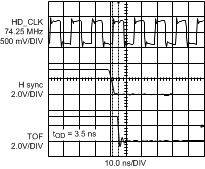
| tD_TOF | TOF Output Delay Time (5) | Specified for any SD or HD format generated from 27-MHz TOF clock (6), outputs initialized (7), 15 pF load | 2 | ns | |||
| CLOCK OUTPUTS (PINS 19, 20, 23, 24) | |||||||
| JitterSD | 27-MHz TIE Peak-to-Peak Output Jitter (8) | HD_CLK = Hi-Z | 23 | ps | |||
| HD_CLK = 74.176 MHz | 40 | ps | |||||
| 67.5-MHz TIE Peak-to-Peak Output Jitter (8) | HD_CLK = Hi-Z | 40 | ps | ||||
| HD_CLK = 74.176 MHz | 50 | ps | |||||
| JitterHD | 74.176-MHz TIE Peak-to-Peak Output Jitter (8) | SD_CLK = Hi-Z | 55 | ps | |||
| SD_CLK = 27 MHz | 65 | ps | |||||
| 74.25-MHz TIE Peak-to-Peak Output Jitter (8) | SD_CLK = Hi-Z | 40 | ps | ||||
| SD_CLK = 27 MHz | 50 | ps | |||||
| 148.35-MHz TIE Peak-to-Peak Output Jitter (8) | SD_CLK = Hi-Z | 60 | ps | ||||
| SD_CLK = 27 MHz | 70 | ps | |||||
| 148.5-MHz TIE Peak-to-Peak Output Jitter (8) | SD_CLK = Hi-Z | 45 | ps | ||||
| SD_CLK = 27 MHz | 55 | ps | |||||
| tD_SD | 27-MHz Output Delay Time (9) | SD_CLK = 27 MHz, Any valid output timing, outputs initialized (7) | 4 | ns | |||
| 67.5-MHz Output Delay Time (9) | SD_CLK = 67.5 MHz, 525i output timing (6), outputs initialized (7) | 6 | ns | ||||
| tD_HD | 74.176-MHz Output Delay Time (10) | HD_CLK = 74.176 MHz, 1080i/59 output timing (6), outputs initialized (7) | 4.5 | ns | |||
| 74.25-MHz Output Delay Time (10) | HD_CLK = 74.25 MHz, 1080i/50 output timing (6), outputs initialized (7) | –0.6 | ns | ||||
| 148.35-MHz Output Delay Time (10) | HD_CLK = 148.35 MHz, 1080p/59 output timing (6), outputs initialized (7) | 1.5 | ns | ||||
| 148.5-MHz Output Delay Time (10) | HD_CLK = 148.5 MHz, 1080p/50 output timing (6), outputs initialized (7) | 4.5 | ns | ||||
| VOD | Differential Signal Output Voltage (11) | 100-Ω differential load | 247 | 350 | 454 | mV | |
| VOS | Common Signal Output Voltage (11) | 100-Ω differential load | 1.125 | 1.250 | 1.375 | V | |
| |VOD| | |Change to VOD| for Complementary Output States (11) | 100-Ω differential load | 50 | |mV| | |||
| |VOS| | |Change to VOS| for Complementary Output States (11) | 100-Ω differential load | 50 | |mV| | |||
| IOS | Output Short Circuit Current | Differential clock output pins connected to GND | 24 | |mA| | |||
| IOZ | Output Hi-Z Leakage Current | Output clock in Hi-Z mode, differential clock output pins connected to VDD or GND | 1 | 10 | |µA| | ||
(1) Typical values represent the most likely parametric norm as determined at the time of characterization. Actual typical values may vary over time and will also depend on the application and configuration. The typical values are not tested and are not ensured on shipped production material.
(2) Limits are 100% production tested at 25°C. Limits over the operating temperature range are specified through correlation using Statistical Quality Control (SQC) methods.
(3) The input voltage to VC_FREERUN (pin 1) should also be within the input range of the external VCXO. The input voltage should be clean from noise that may significantly modulate the VCXO control voltage and consequently produce output jitter during free run operation.
(4) ΔTHV is a required specification that allows for proper frame decoding and subsequent output initialization (alignment). For interlace formats, the H-V sync timing offset must be within ΔTHV for all even fields and be outside ΔTHV for odd fields. For progressive formats, the H-V sync timing offset must be within ΔTHV for all frames. See sections Reference Frame Decoder and Output Frame Line Offset.
(5) tD_TOF is measured from the TOF pulse (leading negative edge) to the 27 MHz SD_CLK output (positive edge) using 50% levels.
(6) For any SD and HD output formats, the TOF pulse can be generated using 27 MHz as the TOF clock by programming TOF_CLK = 0, SD_FREQ = 0, and the alternative output counter values shown in Table 2. See HD Format TOF Generation Using a 27-MHz TOF Clock.
(7) Output initialization refers to the initial alignment of the output frame clock and TOF signals to the input reference frame. See Programming the Output Initialization Sequence.
(8) The SD and HD clock output jitter is based on VCXO clock (pin 29) with 20 ps peak-to-peak using a time interval error (TIE) jitter measurement. The typical TIE peak-to-peak jitter was measured on the LMH1982 evaluation bench board using TDSJIT3 jitter analysis software on a Tektronix DSA70604 oscilloscope and 1 GHz active differential probe. TDSJIT3 Clock TIE Measurement Setup: 10-12 bit error rate (BER), >1 Meg samples recorded using multiple acquisitions Oscilloscope Setup: 20 mV/div vertical scale, 100 µs/div horizontal scale, and 25 GS/s sampling rate
(9) tD_SD is measured from the VCXO clock input (pin 29) to the SD_CLK output (pins 23, 24) using positive edges and 50% levels. The measurement is taken at the leading edge of the TOF pulse, where the input and output clocks are phase aligned at the start of frame.
(10) tD_HD is measured from the VCXO clock input (pin 29) to the HD_CLK output (pins 19, 20) using positive edges and 50% levels. The measurement is taken at the leading edge of the TOF pulse, where the input and output clocks are phase aligned at the start of frame.
(11) This parameter is specified for the SD_CLK output only. This parameter is ensured by design for the HD_CLK output.
6.6 Typical Characteristics
Test conditions: VDD = 3.3V, DVDD = 2.5V, Genlock mode, outputs initialized. H sync and V sync signals to REF_A inputs are from the LMH1981 sync separator, which receives an analog video reference signal from a Tektronix TG700 AVG7/AWVG7 (SD/HD) video signal generator. See the table notes below for register settings (in decimal):
| GNLK = 1, REF_DIV_SEL = 1, FB_DIV = 1716, SD_FREQ = 0, TOF_CLK = 0, TOF_PPL = 1716, TOF_LPFM = 525, REF_LPFM = 525, TOF_OFFSET = 262; all other register settings are default |
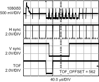
| GNLK = 1, REF_DIV_SEL = 1, FB_DIV = 960, SD_FREQ = 0, HD_FREQ = 0, TOF_CLK = 0, TOF_PPL = 960, TOF_LPFM = 1125, REF_LPFM = 1125, TOF_OFFSET = 562; all other register settings are default |
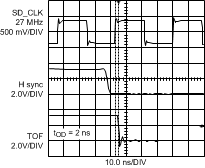
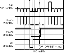
| GNLK = 1, REF_DIV_SEL = 1, FB_DIV = 1728, SD_FREQ = 0, TOF_CLK = 0, TOF_PPL = 1728, TOF_LPFM = 625, REF_LPFM = 625, TOF_OFFSET = 312; all other register settings are default |
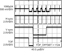
| GNLK = 1, REF_DIV_SEL = 1, FB_DIV = 1000, SD_FREQ = 0, HD_FREQ = 0, TOF_CLK = 0, TOF_PPL = 1000, TOF_LPFM = 1125, REF_LPFM = 1125, TOF_OFFSET = 1124; all other register settings are default |
