SNLS289D April 2008 – September 2015 LMH1982
PRODUCTION DATA.
- 1 Features
- 2 Applications
- 3 Description
- 4 Revision History
- 5 Pin Configuration and Functions
- 6 Specifications
-
7 Detailed Description
- 7.1 Overview
- 7.2 Functional Block Diagram
- 7.3 Feature Description
- 7.4 Device Functional Modes
- 7.5 Programming
- 7.6
Register Maps
- 7.6.1
I2C Interface Control Register Definitions
- 7.6.1.1 Genlock and Input Reference Control Registers
- 7.6.1.2 Genlock Status And Lock Control Register
- 7.6.1.3 Input Control Register
- 7.6.1.4 PLL 1 Divider Register
- 7.6.1.5 PLL 4 Charge Pump Current Control Register
- 7.6.1.6 Output Clock and TOF Control Register
- 7.6.1.7 TOF Configuration Registers
- 7.6.1.8 PLL 1, 2, 3 Charge Pump Current Control Registers
- 7.6.1.9 Reserved Registers
- 7.6.1
I2C Interface Control Register Definitions
-
8 Application and Implementation
- 8.1
Application Information
- 8.1.1 148.35 MHz PLL Initialization Sequence
- 8.1.2 Enabling Genlock Mode
- 8.1.3 Output Disturbance While Output Alignment Mode Enabled
- 8.1.4 Evaluating the LMH1982
- 8.1.5 Input Reference
- 8.1.6 Output Clocks and TOF
- 8.1.7 Reference And Pll Lock Status
- 8.1.8 Loop Response
- 8.2 Typical Applications
- 8.1
Application Information
- 9 Power Supply Recommendations
- 10Layout
- 11Device and Documentation Support
- 12Mechanical, Packaging, and Orderable Information
Package Options
Mechanical Data (Package|Pins)
- RTV|32
Thermal pad, mechanical data (Package|Pins)
- RTV|32
Orderable Information
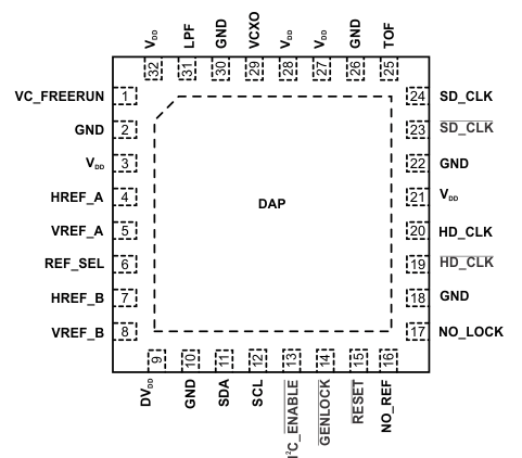
5 Pin Configuration and Functions
RTV Package
32-Pin WQFN
Top View

Pin Functions
| PIN | I/O | SIGNAL LEVEL | DESCRIPTION | |
|---|---|---|---|---|
| NO. | NAME | |||
| – | DAP | — | Supply | Die Attach Pad (Connect to GND) |
| 1 | VC_FREERUN | I | Analog | Free Run Control Voltage Input |
| 2, 10, 18, 22, 26, 30 | GND | — | Supply | Ground |
| 3, 21, 27, 28, 32 | VDD | — | Supply | 3.3-V Supply(1) |
| 4 | HREF_A | I | LVCMOS | H sync Input, Reference A |
| 5 | VREF_A | I | LVCMOS | V sync Input, Reference A |
| 6 | REF_SEL | I | LVCMOS | Reference Select(2)(3) |
| 7 | HREF_B | I | LVCMOS | H sync Input, Reference B |
| 8 | VREF_B | I | LVCMOS | V sync Input, Reference B |
| 9 | DVDD | — | Supply | 2.5-V Supply(4) |
| 11 | SDA | I/O | I2C | I2C Data(5) |
| 12 | SCL | I | I2C | I2C Clock(5) |
| 13 | I2C_ENABLE | I | LVCMOS | I2C Enable |
| 14 | GENLOCK | I | LVCMOS | Mode Select(6) |
| 15 | RESET | I | LVCMOS | Device Reset |
| 16 | NO_REF | O | LVCMOS | Reference Status Flag |
| 17 | NO_LOCK | O | LVCMOS | Lock Status Flag |
| 19, 20 | HD_CLK, HD_CLK | O | LVDS | HD Clock Output |
| 23, 24 | SD_CLK, SD_CLK | O | LVDS | SD Clock Output |
| 25 | TOF | O | LVCMOS | Top of Frame Pulse |
| 29 | VCXO | I | LVCMOS | VCXO Clock Input |
| 31 | LPF | O | Analog | VCXO PLL Loop Filter |
(1) Refer to Power Supply Sequencing.
(2) To control reference selection via the REF_SEL pin instead of the I2C interface (default), program I2C_RSEL = 0 (register 00h).
(3) To override reference control through pin 6 and instead use pin 6 as an logic input for output initialization, program PIN6_OVRD = 1 (register 02h); accordingly, the TOF_INIT bit (register 0Ah) will be ignored and reference selection must be controlled through I2C.
(4) Must be ≤ VDD + 0.3 V. Refer to Power Supply Sequencing.
(5) SDA and SCL pins each require a 4.7-kΩ (typical) pullup resistor to the VDD supply.
(6) To control mode selection through the GENLOCK pin instead of the I2C interface (default), program I2C_GNLK = 0 (register 00h).