SNLS309I April 2010 – December 2014 LMH1983
PRODUCTION DATA.
- 1 Features
- 2 Applications
- 3 Description
- 4 Revision History
- 5 Description (continued)
- 6 Pin Configurations and Functions
- 7 Specifications
-
8 Detailed Description
- 8.1 Overview
- 8.2 Functional Block Diagram
- 8.3
Feature Description
- 8.3.1 Control of PLL1
- 8.3.2 PLL1 Loop Response Design Equations
- 8.3.3 Control of PLL2 and PLL3
- 8.3.4 Control of PLL4
- 8.3.5 Clock Output Jitter
- 8.3.6 Lock Determination
- 8.3.7 Lock Time Considerations
- 8.3.8 LOR Determination
- 8.3.9 Output Driver Adjustments
- 8.3.10 TOF1 Alignment
- 8.3.11 TOF2 and TOF3 Alignment
- 8.3.12 TOF4 Alignment
- 8.4 Device Functional Modes
- 8.5 Programming
- 8.6 Register Map
- 9 Applications and Implementation
- 10Power Supply Recommendations
- 11Layout
- 12Device and Documentation Support
- 13Mechanical, Packaging, and Orderable Information
Package Options
Mechanical Data (Package|Pins)
- RTA|40
Thermal pad, mechanical data (Package|Pins)
- RTA|40
Orderable Information
9 Applications and Implementation
NOTE
Information in the following applications sections is not part of the TI component specification, and TI does not warrant its accuracy or completeness. TI’s customers are responsible for determining suitability of components for their purposes. Customers should validate and test their design implementation to confirm system functionality.
9.1 Application Information
The LMH1983 is an analog phase locked loop (PLL) clock generator that can output simultaneous clocks at a variety of video and audio rates, synchronized or “genlocked” to Hsync and Vsync input reference timing. The LMH1983 features an output Top of Frame (TOF) pulse generator for each of its four channels, each with programmable timing that can also be synchronized to the reference frame. The clock generator uses a two-stage PLL architecture to attenuate input timing jitter for minimum jitter transfer. The combination of the external VCXO, external loop filter, and programmable PLL parameters provides flexibility to optimize the loop bandwidth and loop response for design applications.
9.2 Typical Applications
9.2.1 Typical Genlock Timing Generation with NTSC 525i/29.97 High Speed Reference
The LMH1983 is commonly used with Hsync, Vsync, and Fsync timing signals as a reference for genlock. Once these signals are provided, the LMH1983 can produce a specific set of clock output signals required by a downstream endpoint. In some video applications, a multi-format video sync separator is used to derive the Hsync, Vsync, and Fsync signals from a standard analog SD/ED/HD video signal. In Figure 22, a LMH1981 multi-format sync separator is used to provide HIN, VIN, and FIN for the LMH1983. In this case, LMH1983 PLLs 1-4 provide a 27 MHz/29.97 Hz, 148.5 MHz/29.97 Hz, 148.35 MHz/59.94 Hz, and 24.576 MHz/5.994 Hz output, respectively, to an A/V Frame Synchronizer. Another example of this application can be seen in Figure 23, where HIN, VIN, and FIN signals are provided directly from an FPGA SDI RX without a sync separator. In the latter example, the NTSC 525i/29.97 HIN, VIN, and FIN parameters are provided individually for the LMH1983, after which the LMH1983 provides 3G, 3G/1.001, and Audio Clock Generation.
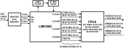 Figure 22. LMH1983 Video Genlock Timing Generation for A/V Frame Synchronizer
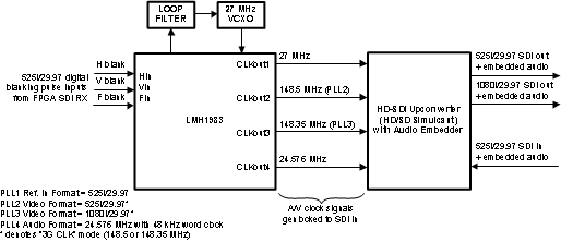 Figure 23. LMH1983 Video Timing Generation for HD-SDI Up-Conversion with Audio Embed/De-embed
9.2.1.1 Design Requirements
When designing for the LMH1983, it is essential to choose the correct VCXO and external loop filter capacitors. The following subsections provide guidance regarding how to select these components to improve timing stability and accuracy.
9.2.1.1.1 VCXO Selection Criteria
The recommended VCXO is CTS part number 357LB3C027M0000, which has an absolute pull range of ±50 ppm and a temperature range of –20°C to +70°C. A VCXO with a smaller APR can provide better frequency stability and slightly lower jitter, but the APR must be larger than the anticipated variation of the input frequency range.
9.2.1.1.2 Loop Filter Capacitors
The most common types of capacitors used in many circuits today are ferroelectric ceramic capacitors such as X7R, Y5V, X5R, Y5U, and so on. These capacitors suffer from piezoelectric effects, which generate an electrical signal in response to mechanical vibration, stress, and shock. This effect can adversely affect the jitter performance when presented to the control input to the VCXO. The easiest way to eliminate this effect is to use tantalum capacitors that do not exhibit the piezoelectric effect.
9.2.1.2 Detailed Design Procedure
Once the appropriate external VCXO and loop filter components are selected, the input timing signaling should be referenced to Table 2 to determine whether NTSC 525i/29.97 sync format is supported. This video format is a supported video format for automatic detection under Auto Format Detection Code 0, so it is not necessary to override the input auto-detection feature.
Once PLL1 has genlocked to the chosen NTSC, 525i input reference signal, PLLs 2-3 can be set according to the desired output signals specified in Figure 23. Refer to Table 6 and Table 7 for a list of possible input and output formats available for auto-format detection in Figure 22 and Figure 23, respectively. The format code can be applied as an expected input format for PLL1 (Register 0x20) or a programmed output format for PLL2 (Register 0x07) and PLL3 (Register 0x08).
Table 6. Relevant Auto-Format Detection Codes for Figure 22
| PLLx (INPUT/OUTPUT) |
FORMAT CODE | DESCRIPTION | HSync PERIOD (in 27 MHz CLOCKS) |
|---|---|---|---|
| PLL1 (Input) | 0 | 525I29.97 | 1716 |
| PLL2 (Output) | 0 | 525I29.97 | 1716 |
| PLL3 (Output) | 13 | 1080P59.94 | 400.4 |
Table 7. Relevant Auto-Format Detection Codes for Figure 23
| PLLx (INPUT/OUTPUT) |
FORMAT CODE | DESCRIPTION | HSync PERIOD (in 27 MHz CLOCKS) |
|---|---|---|---|
| PLL1 (Input) | 0 | 525I29.97 | 1716 |
| PLL2 (Output) | 0 | 525I29.97 | 1716 |
| PLL3 (Output) | 21 | 1080I29.97 | 800.8 |
To ensure correct auto-detection and CLKout signaling desired in Figure 22 and Figure 23, the following SMBus register values should be verified or changed from their default values.
Table 8. SMBus Register Settings for Figure 22
| Register[Bit(s)] | WRITE VALUE | COMMENTS |
|---|---|---|
| 0x05[5] | 1'b | Auto Format Detect enabled |
| 0x05[4:3] | 01'b | PLL1 operating in Genlock mode |
| 0x05[1] | 1'b | Forces PLL2 = 148.5 MHz and PLL3 = 148.35 MHz |
| 0x07[5:0] | 000000'b | Set PLL2 Output to Format Detection Code 0 (0x00) |
| 0x08[5:0] | 001101'b | Set PLL3 Output to Format Detection Code 13 (0x0D) |
| 0x11[5:4] | 10'b | Set to always align when misaligned |
| 0x11[3:2] | 01'b | Drift lock (small misalignment), crash lock (large misalignment) |
| 0x12[5:4] | 10'b | Set TOF2 to always align when misaligned |
| 0x13[5:4] | 10'b | Set TOF3 to always align when misaligned |
| 0x14[5:4] | 10'b | Set AFS_Align_Mode to always align when misaligned |
| 0x34[7:4] | 0010'b | Set PLL4_DIV to divide-by-4 for 24.576 MHz |
Table 9. SMBus Register Settings for Figure 23
| Register[Bit(s)] | WRITE VALUE | COMMENTS |
|---|---|---|
| 0x05[5] | 1'b | Auto Format Detect enabled |
| 0x05[4:3] | 01'b | PLL1 operating in Genlock mode |
| 0x05[1] | 1'b | Forces PLL2 = 148.5 MHz and PLL3 = 148.35 MHz |
| 0x07[5:0] | 000000'b | Set PLL2 Output to Format Detection Code 0 (0x00) |
| 0x08[5:0] | 010101'b | Set PLL3 Output to Format Detection Code 21 (0x15) |
| 0x11[5:4] | 10'b | Set to always align when misaligned |
| 0x11[3:2] | 01'b | Drift lock (small misalignment), crash lock (large misalignment) |
| 0x12[5:4] | 10'b | Set TOF2 to always align when misaligned |
| 0x13[5:4] | 10'b | Set TOF3 to always align when misaligned |
| 0x14[5:4] | 10'b | Set AFS_Align_Mode to always align when misaligned |
| 0x34[7:4] | 0010'b | Set PLL4_DIV to divide-by-4 for 24.576 MHz |
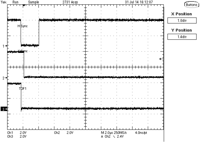
9.2.1.3 Application Curves
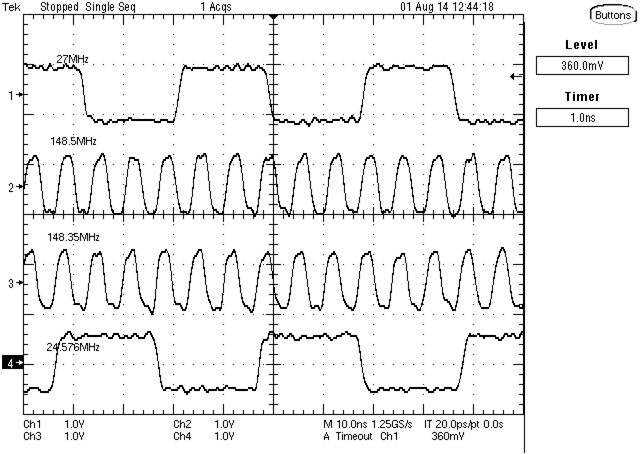
| 10 ns / div | ||
| Traces 1-4: 1V / div | ||
| 20 µs / div | ||
| Traces 1-3: 2 V / div | ||
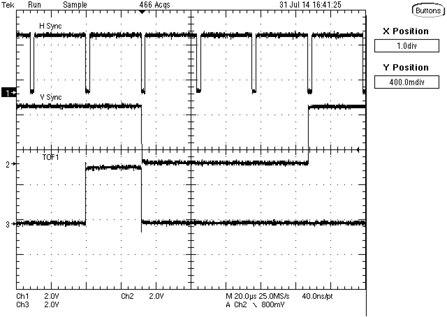
| 20 µs / div | ||
| Traces 1-3: 2V / div | ||
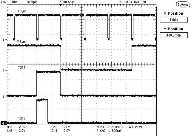
| 20 µs / div | ||
| Traces 1-4: 2 V / div | ||
9.2.2 A/V Clock Generation with Recognized Clock-based Input Reference
The LMH1983 is shown in the following application example where the HIN input reference timing signal is clock-based. After achieving genlock, the LMH1983 can produce a specific set of clock output signals required downstream. In this case, LMH1983 PLLs 1-4 provide a 27 MHz, 74.25 MHz, 74.176 MHz, and 98.304 MHz output, respectively.
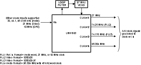 Figure 28. LMH1983 A/V Clock Generation with Non-Format Specific Input Clock Reference
9.2.2.1 Design Requirements
When designing for the LMH1983, it is essential to ensure that the correct VCXO and external loop filter capacitors are chosen. Refer to VCXO Selection Criteria and Loop Filter Capacitors for guidance regarding how to select these components to improve timing stability and accuracy.
9.2.2.2 Detailed Design Procedure
Once the appropriate external VCXO and loop filter components are selected, the input timing signaling should be referenced to the "Supported Formats Lookup Table (LUT)" (see Table 2) to determine whether the video clock, GPS clock, and audio clock are supported by automatic format detection. From Table 2 and the Auto Format Detection Codes, all of the reference clock inputs mentioned in this application are supported under the auto format detection feature. Once PLL1 has genlocked to the chosen HIN signal, PLLs 2-3 can be set according to the desired output signals specified in Auto Format Detection Codes. Refer to Table 10 for a list of possible input and output formats available for auto-format detection in this application. The format code can be applied as an expected input format for PLL1 (Register 0x20) or a programmed output format for PLL2 (Register 0x07) and PLL3 (Register 0x08).
Table 10. Relevant Auto-Format Detection Codes for Figure 28
| PLLx (INPUT/OUTPUT) | FORMAT CODE | DESCRIPTION | HSync PERIOD (in 27 MHz CLOCKS) |
|---|---|---|---|
| PLL2 (Output) | 22 | 1080I25 | 960 |
| PLL3 (Output) | 21 | 1080I29.97 | 800.8 |
| PLL1 (Input) | 25 | 48 kHz Audio | 562.5 |
| PLL1 (Input) | 26 | 96 kHz Audio | 281.25 |
| PLL1 (Input) | 27 | 44.1 kHz Audio | 612.244898 |
| PLL1 (Input) | 28 | 32 kHz Audio | 843.75 |
| PLL1 (Input) | 29 | 27 MHz HSync | 1 |
| PLL1 (Input) | 30 | 10 MHz HSync | 2.7 |
To ensure correct auto-detection and the correct CLKout signaling desired in Figure 28, the following SMBus register values should be verified or changed from their default values.
Table 11. SMBus Register Settings for Figure 28
| REGISTER[Bit(s)] | WRITE VALUE | COMMENTS |
|---|---|---|
| 0x05[5] | 1'b | Auto Format Detect enabled |
| 0x05[4:3] | 01'b | PLL1 operating in Genlock mode |
| 0x05[1] | 0'b | Allow PLL2 and PLL3 to use the native clock rates |
| 0x07[5:0] | 010110'b | Set PLL2 Output to Format Detection Code 22 (0x16) |
| 0x08[5:0] | 010101'b | Set PLL3 Output to Format Detection Code 21 (0x15) |
| 0x11[5:4] | 10'b | Set to always align when misaligned |
| 0x11[3:2] | 01'b | Drift lock (small misalignment), crash lock (large misalignment) |
| 0x12[5:4] | 10'b | Set TOF2 to always align when misaligned |
| 0x13[5:4] | 10'b | Set TOF3 to always align when misaligned |
| 0x14[5:4] | 10'b | Set AFS_Align_Mode to always align when misaligned |
| 0x2E[4] | 1'b | Set PLL2_DIV to divide-by-2 for 74.25 MHz |
| 0x31[4] | 1'b | Set PLL3_DIV to divide-by-2 for 74.176 MHz |
| 0x34[7:4] | 0000'b | Set PLL4_DIV to divide-by-1 for 98.304 MHz |
9.2.2.3 Application Curve
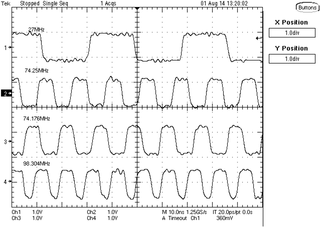
| 10ns / div | ||
| Traces 1-4: 1V / div | ||
9.2.3 A/V Clock Generation Using Free-Run Mode
The LMH1983 can be used in free-run mode, as shown in the following application example. No HIN, VIN, and FIN input reference timing signals are provided. Instead, the LMH1983 tracks a 27 MHz TCXO reference, which replaces the external VCXO and loop filter mentioned in previous applications. The LMH1983 can still produce a specific set of clock output signals required by a downstream endpoint. In this application, LMH1983 PLLs 1-4 provide a 27 MHz, 148.5 MHz, 148.35 MHz, and 98.304 MHz output, respectively.
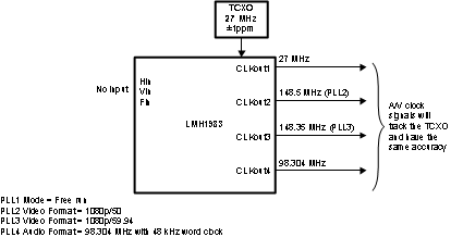 Figure 30. High-Precision, Stable A/V Clock Generation Using a 27 MHz TCXO Reference
9.2.3.1 Design Requirements
This application requires less components than the previous applications mentioned in this section. This is because there is no HIN reference, external VCXO, or loop filter. However, the PLL1 signal is still applied via the 27 MHz TCXO clock signal on the XOin± pins. Using a TCXO for reference allows a stable, standalone clock generation for PLLs 2-4.
9.2.3.2 Detailed Design Procedure
Since no HIN input timing signaling is provided, this application example cannot use the "Supported Formats Lookup Table (LUT)" (see Table 2) for automatic format detection. However, PLLs 2-4 can still be manually programmed to output the correct output format using Auto Format Detection Codes. To output the desired video and audio formats from PLLs 2-3, the following output codes should be used:
Table 12. Auto-Format Detection Output Codes for Figure 30
| PLLx (INPUT/OUTPUT) | FORMAT CODE | DESCRIPTION | HSync PERIOD (in 27 MHz CLOCKS) |
|---|---|---|---|
| PLL2 (Output) | 14 | 1080P50 | 480 |
| PLL3 (Output) | 13 | 1080P59.94 | 400.4 |
To ensure correct auto-detection and the correct CLKout signaling desired in Figure 30, the following SMBus register values should be verified or changed from their default values.
Table 13. SMBus Register Settings for Figure 30
| REGISTER[Bit(s)] | WRITE VALUE | COMMENTS |
|---|---|---|
| 0x05[5] | 1'b | Auto Format Detect enabled |
| 0x05[4:3] | 00'b | PLL1 operating in Free-run mode |
| 0x05[1] | 1'b | Forces PLL2 = 148.5 MHz and PLL3 = 148.35 MHz |
| 0x07[5:0] | 001110'b | Set PLL2 Output to Format Detection Code 14 (0x0E) |
| 0x08[5:0] | 001101'b | Set PLL3 Output to Format Detection Code 13 (0x0D) |
| 0x11[5:4] | 10'b | Set to always align when misaligned |
| 0x11[3:2] | 01'b | Drift lock (small misalignment), crash lock (large misalignment) |
| 0x12[5:4] | 10'b | Set TOF2 to always align when misaligned |
| 0x13[5:4] | 10'b | Set TOF3 to always align when misaligned |
| 0x34[7:4] | 0000'b | Set PLL4_DIV to divide-by-1 for 98.304 MHz |
9.2.3.3 Application Curve
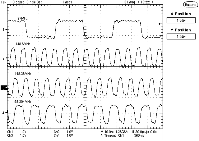
| 10 ns / div | ||
| Traces 1-4: 1 V / div | ||