SNLS309I April   2010  – December 2014 LMH1983

PRODUCTION DATA.  

  1. Features
  2. Applications
  3. Description
  4. Revision History
  5. Description (continued)
  6. Pin Configurations and Functions
  7. Specifications
    1. 7.1 Absolute Maximum Ratings
    2. 7.2 ESD Ratings
    3. 7.3 Recommended Operating Conditions
    4. 7.4 Thermal Information
    5. 7.5 Electrical Characteristics
    6. 7.6 Frame Timing Outputs Timing Requirements
    7. 7.7 Frame Timing Outputs Switching Characteristics
    8. 7.8 Typical Characteristics
  8. Detailed Description
    1. 8.1 Overview
    2. 8.2 Functional Block Diagram
    3. 8.3 Feature Description
      1. 8.3.1  Control of PLL1
      2. 8.3.2  PLL1 Loop Response Design Equations
      3. 8.3.3  Control of PLL2 and PLL3
      4. 8.3.4  Control of PLL4
      5. 8.3.5  Clock Output Jitter
      6. 8.3.6  Lock Determination
      7. 8.3.7  Lock Time Considerations
      8. 8.3.8  LOR Determination
      9. 8.3.9  Output Driver Adjustments
      10. 8.3.10 TOF1 Alignment
      11. 8.3.11 TOF2 and TOF3 Alignment
        1. 8.3.11.1 TOF3 Initialization Set Up
      12. 8.3.12 TOF4 Alignment
    4. 8.4 Device Functional Modes
      1. 8.4.1 Reference Detection
      2. 8.4.2 User Defined Formats
      3. 8.4.3 Auto Format Detection Codes
      4. 8.4.4 Free-Run, Genlock, and Holdover Modes
    5. 8.5 Programming
      1. 8.5.1 I2C Interface Protocol
      2. 8.5.2 Write Sequence
      3. 8.5.3 Read Sequence
    6. 8.6 Register Map
  9. Applications and Implementation
    1. 9.1 Application Information
    2. 9.2 Typical Applications
      1. 9.2.1 Typical Genlock Timing Generation with NTSC 525i/29.97 High Speed Reference
        1. 9.2.1.1 Design Requirements
          1. 9.2.1.1.1 VCXO Selection Criteria
          2. 9.2.1.1.2 Loop Filter Capacitors
        2. 9.2.1.2 Detailed Design Procedure
        3. 9.2.1.3 Application Curves
      2. 9.2.2 A/V Clock Generation with Recognized Clock-based Input Reference
        1. 9.2.2.1 Design Requirements
        2. 9.2.2.2 Detailed Design Procedure
        3. 9.2.2.3 Application Curve
      3. 9.2.3 A/V Clock Generation Using Free-Run Mode
        1. 9.2.3.1 Design Requirements
        2. 9.2.3.2 Detailed Design Procedure
        3. 9.2.3.3 Application Curve
  10. 10Power Supply Recommendations
  11. 11Layout
    1. 11.1 Layout Guidelines
    2. 11.2 Layout Example
  12. 12Device and Documentation Support
    1. 12.1 Documentation Support
      1. 12.1.1 Related Documentation
    2. 12.2 Trademarks
    3. 12.3 Electrostatic Discharge Caution
    4. 12.4 Glossary
  13. 13Mechanical, Packaging, and Orderable Information

Package Options

Mechanical Data (Package|Pins)
Thermal pad, mechanical data (Package|Pins)
Orderable Information

10 Power Supply Recommendations

It is important to ensure that the LMH1983 is provided with an adequate power supply that provides the cleanest voltage to the VDD_IO and VDD supply pins. One potential source of jitter on a multiple clock system such as the LMH1983 is interference among the four PLLs on the chip. To help reduce this effect, each PLL is run from a separate power supply internally on the LMH1983, and each supply has its own internal regulator. These regulators each require their own external bypass as seen in Figure 32 with bypass capacitors.

power_supply_rec.gif
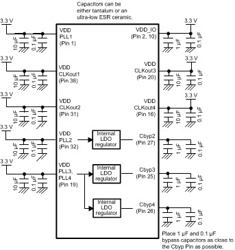
Figure 32. LMH1983 Power Supply Connection Diagram