SNLS309I April 2010 – December 2014 LMH1983
PRODUCTION DATA.
- 1 Features
- 2 Applications
- 3 Description
- 4 Revision History
- 5 Description (continued)
- 6 Pin Configurations and Functions
- 7 Specifications
-
8 Detailed Description
- 8.1 Overview
- 8.2 Functional Block Diagram
- 8.3
Feature Description
- 8.3.1 Control of PLL1
- 8.3.2 PLL1 Loop Response Design Equations
- 8.3.3 Control of PLL2 and PLL3
- 8.3.4 Control of PLL4
- 8.3.5 Clock Output Jitter
- 8.3.6 Lock Determination
- 8.3.7 Lock Time Considerations
- 8.3.8 LOR Determination
- 8.3.9 Output Driver Adjustments
- 8.3.10 TOF1 Alignment
- 8.3.11 TOF2 and TOF3 Alignment
- 8.3.12 TOF4 Alignment
- 8.4 Device Functional Modes
- 8.5 Programming
- 8.6 Register Map
- 9 Applications and Implementation
- 10Power Supply Recommendations
- 11Layout
- 12Device and Documentation Support
- 13Mechanical, Packaging, and Orderable Information
Package Options
Mechanical Data (Package|Pins)
- RTA|40
Thermal pad, mechanical data (Package|Pins)
- RTA|40
Orderable Information
11 Layout
11.1 Layout Guidelines
When designing the PCB layout for the LMH1983, it is important to follow these the guidelines:
- Whenever possible, dedicate an entire layer to each power supply. This will reduce the inductance in the supply plane.
- Use surface mount components whenever possible.
- Place bypass capacitors and filter components as close as possible to each power pin.
- Place the loop filter components, including the buffer amplifier, and VCXO as close as possible to the LMH1983.
- Do not allow discontinuities in the ground planes – return currents follow the path of least resistance. For high frequency signals this will be the path of least inductance.
- Make sure to match the trace lengths of all differential traces.
- Remember that vias have significant inductance — when using a via to connect to a power supply or ground layer, two in parallel will reduce the inductance over a single via.
- Connect the pad on the bottom of the package to a solid ground connection. This contact is used as a major ground connection as well as providing a thermal conduit which helps to maintain a constant die temperature.
- See Application Note: AN-1187, Leadless Leadframe Package (LLP) (SNOA401) for more Information on the LLP (WQFN) style package.
11.2 Layout Example
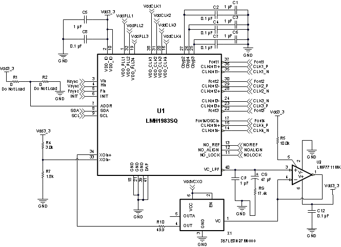 Figure 33. LMH1983 Typical Interface Circuit
An example of a typical application circuit for the LMH1983 is shown in the Figure 33. When performing PCB layout, key areas to consider regarding this circuit are the loop filter – which consists of RS, CS, CP and the LM7711 Operational Amplifier which buffers the loop filter output prior to driving the control voltage input of the VCXO. Care must be taken in the component selection for the loop filter components (see VCXO Selection Criteria and Loop Filter Capacitors). The CLKout outputs are differential LVDS signals and should be treated as differential signals. These signals may be laid out as fully differential lines, in which the characteristic impedance between the two lines is nominally 100 Ω. Alternately, loosely coupled lines may be used, in which case the characteristic impedance of each line should be 50 Ω referenced to GND. In either case, care should be taken to match the lengths of the traces as closely as possible. Trace length mismatches on a differential line will add to the jitter seen on that line. Jitter is also added to the clock outputs if other signals are allowed to interfere with the signal traces. Therefore, to the greatest extent possible, the clock traces should be isolated from other signals. Long parallel runs should also be avoided. In places where a hostile signal must cross a sensitive clock signal, it should be routed such that it crosses as closely as possible to a 90° crossing.
When performing board layouts with the LMH1983, stencil parameters such as aperture area ratio and the fabrication process have a significant impact on paste deposition. Inspection of the stencil prior to placement of the WQFN package is highly recommended to improve board assembly yields. If the via and aperture openings are not carefully monitored, the solder may flow unevenly through the DAP. Stencil parameters for aperture opening and via locations are shown in Figure 34.
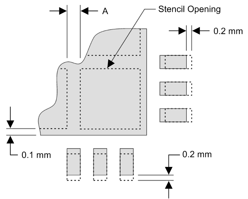 Figure 34. No Pullback LLP, Single Row Reference Diagram
Table 14. No Pullback LLP Stencil Aperture Summary for LMH1983
| DEVICE | PIN COUNT |
MKT. DWG. | PCB I/O PAD SIZE (mm) |
PCB PITCH (mm) |
PCB DAP SIZE (mm) |
STENCIL I/O APERTURE (mm) |
STENCIL DAP APERTURE (mm) |
NUMBER of DAP APERTURE OPENINGS |
GAP BETWEEN DAP APERTURE (DIM A mm) |
|---|---|---|---|---|---|---|---|---|---|
| LMH1983 | 40 | SNA40A | 0.25 x 0.6 | 0.5 | 4.6 x 4.6 | 0.25 x 0.7 | 1.0 x 1.0 | 16 | 0.2 |
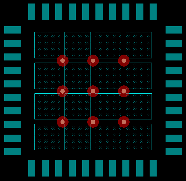 Figure 35. 40-Pin WQFN Stencil Example of Via and Opening Placement
The following PCB layout example is derived from the layout design of the LMH1983 in the SD1983EVK Evaluation Module User's Guide (SNLU001). This graphic and additional layout board description demonstrates both proper routing and solder techniques when designing in this clock generator.
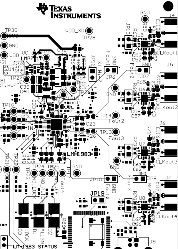 Figure 36. LMH1983 Example Layout