SNLS309I April 2010 – December 2014 LMH1983
PRODUCTION DATA.
- 1 Features
- 2 Applications
- 3 Description
- 4 Revision History
- 5 Description (continued)
- 6 Pin Configurations and Functions
- 7 Specifications
-
8 Detailed Description
- 8.1 Overview
- 8.2 Functional Block Diagram
- 8.3
Feature Description
- 8.3.1 Control of PLL1
- 8.3.2 PLL1 Loop Response Design Equations
- 8.3.3 Control of PLL2 and PLL3
- 8.3.4 Control of PLL4
- 8.3.5 Clock Output Jitter
- 8.3.6 Lock Determination
- 8.3.7 Lock Time Considerations
- 8.3.8 LOR Determination
- 8.3.9 Output Driver Adjustments
- 8.3.10 TOF1 Alignment
- 8.3.11 TOF2 and TOF3 Alignment
- 8.3.12 TOF4 Alignment
- 8.4 Device Functional Modes
- 8.5 Programming
- 8.6 Register Map
- 9 Applications and Implementation
- 10Power Supply Recommendations
- 11Layout
- 12Device and Documentation Support
- 13Mechanical, Packaging, and Orderable Information
Package Options
Mechanical Data (Package|Pins)
- RTA|40
Thermal pad, mechanical data (Package|Pins)
- RTA|40
Orderable Information
8 Detailed Description
8.1 Overview
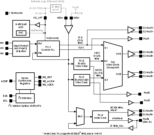
The LMH1983 is an analog phase locked loop (PLL) clock generator that can output simultaneous clocks at a variety of video and audio rates, synchronized or “genlocked” to Hsync and Vsync input reference timing. The LMH1983 features an output Top of Frame (TOF) pulse generator for each of its four channels, each with programmable timing that can also be synchronized to the reference frame. The clock generator uses a two-stage PLL architecture. The first stage is a VCXO-based PLL (PLL1) that requires an external 27 MHz VCXO and loop filter. In Genlock mode, PLL1 can phase lock a low loop bandwidth VCXO clock to the input reference. The VCXO provides a low phase noise clock source to attenuate input timing jitter for minimum jitter transfer. The combination of the external VCXO, external loop filter, and programmable PLL parameters provide flexibility for the system designer to optimize the loop bandwidth and loop response for the application.
The second stage consists of three PLLs (PLL2, PLL3, PLL4) with integrated VCOs and loop filters. These PLLs continually track the reference VCXO clock phase from PLL1 regardless of the device mode. The PLL2 and PLL3 have pre-configured divider ratios to provide frequency multiplication or translation from the VCXO clock frequency to generate the two common HD clock rates (148.5 MHz and 148.35 MHz). PLL4 is pre-configured to generate an audio clock that defaults to a 24.576 MHz output, although PLL4 has several registers that allow it to be re-configured for a variety of applications.
The VCO PLLs use a high loop bandwidth to assure PLL stability, so the VCXO of PLL1 must provide a stable low-jitter clock reference to ensure optimal output jitter performance. Any unused clock or TOF output can be placed in Hi-Z mode. This may be useful for reducing power dissipation as well as reducing jitter or phase noise on the active clock output. The TOF pulse can be programmed to indicate the start (top) of frame and even provide format cross-locking. The output format registers should be programmed to specify the output timing (output clocks and TOF pulse), the output timing offset relative to the reference, and the output initialization (alignment) to the reference frame.
When a loss of reference occurs during genlock, PLL1 can default to either Free-run or Holdover operation. When Free-run is selected, the output frequency accuracy will be determined by the external bias on the free-run control voltage input pin, VC_LPF. When Holdover is selected, the loop filter can hold the control voltage to maintain short-term output phase accuracy for a brief period in order to allow the application to select the secondary input reference and re-lock the outputs. These options in combination with a proper PLL1 loop response design can provide flexibility to manage output clock behavior during loss and re-acquisition of the reference. The reference status and PLL lock status flags can provide real-time status indication to the application system. The loss of reference and lock detection thresholds can also be configured.
8.2 Functional Block Diagram
8.3 Feature Description
The following subsections provide information about the various control mechanisms and features that are fundamental to the LMH1983 clock generator.
8.3.1 Control of PLL1
PLL1 generates a 27 MHz reference that is used as the primary frequency reference for all of the other PLLs in the device. PLL1 has a dual loop architecture with the primary loop locking the external 27 MHz VCXO to a harmonic of the HIN signal. In addition to this loop, there is a secondary loop that may be used in genlock operations. This second loop compares the phase of the TOF1 output signal from the LMH1983 to the FIN signal. In order to bring the frame alignment of the output signals into sync with the input reference, the second loop may override the primary loop. Detailed information about controlling this functionality is described in TOF1 Alignment.
To illustrate the dual loop architecture of PLL1, refer to the PLL1 block diagram in Figure 9. The primary loop takes the reference applied to the HIN input and divides that by R (stored in Registers 0x29 and 0x2A). The dividend is then compared in phase and frequency to the output of the external 27 MHz VCXO divided by N (stored in Registers 0x2B and 0x2C). The PFD (phase frequency detector) then generates output pulses that are integrated via an external loop filter that drives the control voltage of the external VCXO.
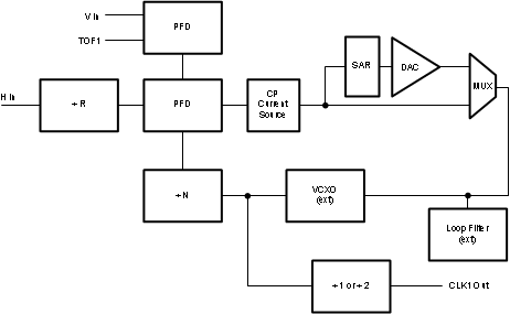 Figure 9. PLL1 Block Diagram
Since PLL2, PLL3, and PLL4 all use PLL1 as their input reference, the performance of PLL1 affects the performance of all four clock outputs. The loop filters for the other three PLLs are internal, and the bandwidths are set significantly higher than that of PLL1, so the low frequency jitter characteristics of all four clock outputs are determined by the loop response of PLL1. Accordingly, special attention should be paid to the PLL1's loop bandwidth and damping factor.
8.3.2 PLL1 Loop Response Design Equations
The loop response is primarily determined by the loop filter components and the loop gain. A passive second order loop filter consisting of RS, CS, and CP components can provide sufficient input jitter attenuation for most applications. In some cases, a higher order filter may be used to shape the low frequency response of PLL1 further. Assuming a topology for the loop filter similar to that shown in the Figure 9, the bandwidth of the PLL is determined by:
where
- RS is the series resistor value in the external loop filter.
- KVCO is the nominal 27 MHz VCXO gain in Hz/V. KVCO= Pull_range*27 MHz/Vin_Range. For the VCXO used in the typical interface circuit (Mfgr: CTS, P/N 357LB3C027M0000): LVCO=100 ppm*27 MHz / (3.0V-0.3V) = 1000 Hz/V
- ICP1 is the current from the PLL1 charge pump.
- FB_DIV is the divide ratio of the PLL, which is set by the R and N register values, this will be equal to the number of 27 MHz clock pulses in one HIN period. For NTSC, this value will be 1716.
Under normal operation, several of these parameters are set by the device automatically, for example the charge pump current and the value of 'FB_DIV'. When the input reference format changes, both N and the charge pump current are updated, N is changed to allow for lock to the new reference, and the charge pump current is adjusted to maintain constant loop bandwidth.
It should be noted that this bandwidth calculation is an approximation and does not take into account the effects of the damping factor or the second pole introduced by CP.
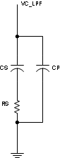 Figure 10. External Loop Filter Schematic Detail
At frequencies far above the –3dB loop bandwidth, the closed-loop frequency response of PLL1 will roll off at about –40dB/decade, which is useful for attenuating input jitter at frequencies above the loop bandwidth. Near the –3dB corner frequency, the roll-off characteristic depends on other factors, such as damping factor and filter order.
To prevent output jitter due to the modulation of the VCXO by the PLL's phase comparison frequency, the bandwidth needs to meet the following criterion:
PLL1's damping factor can be approximated by:
where
- CS is the value of the series capacitor (in Farads)
Typically, DF is targeted to be between 1/√2 and 1, which will yield a good trade-off between lock time and reference spur attenuation. DF is related to the phase margin, a measure of the PLL stability.
There is a second parallel capacitor, CP, which is needed to filter the reference spurs introduced by the PLL. The spurs may modulate the VCXO control voltage, leading to jitter. The following relationship should be used to determine CP:
The PLL loop gain, K, can be calculated as:
Therefore, Bandwidth and Damping Factor can be expressed in terms of K:
8.3.3 Control of PLL2 and PLL3
PLL2 and PLL3 have the least amount of flexibility of the four PLLs in the LMH1983. They are pre-programmed to run at 148.5 MHz and 148.35 MHz respectively. There is a divide-by-two option available to allow the output to be 74.25 MHz or 74.18 MHz, should these frequencies be required. These two PLLs can also be disabled – disabling PLL2 or PLL3 can save significant amounts of power if that particular clock is not required. Figure 11 shows a simplified functional block diagram of PLL2 and PLL3.
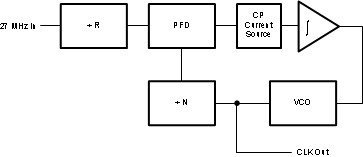 Figure 11. PLL2 / PLL3 Block Diagram
8.3.4 Control of PLL4
Although originally intended to generate only a clock for audio use, PLL4 features much greater versatility. Several registers may be used to configure PLL4 to generate a broad selection of frequencies. The default state for PLL4 is to generate 24.576 MHz (48 kHz x 512) on the output of CLK4 and a 5.996 Hz output from TOF4. This is done by taking CLK1 (27 MHz), and dividing by 75, resulting in a signal of 360 kHz. This frequency is compared to the internal PLL4 VCO, nominally 1.2 GHz, divided by 4096. The VCO frequency is adjusted via register control until the resulting frequency yields 360 kHz. The final VCO frequency is then divided by 12 to generate a 98.304 MHz signal (48 kHz x 2048). Any power of two multiple of 48 kHz can be generated by changing the contents of the PLL4_DIV component of Register 0x34. Note that the divider here is in powers of 2, so the default value of 2 results in the 98.304 MHz signal being divided by 22 or 4. The final CLKout4 frequency is therefore 24.576 MHz. PLL4_DIV is a 4-bit value, so values up to 15 may be programmed, resulting in a divide by 215 or 32,768. If audio clocks based on a 44.1 kHz sampling clock are desired, refer to Application Note AN–2108, Generating 44.1 kHz Based Clocks with the LMH1983, (SNLA129) for detailed instructions.
TOF4 has two different operation modes. When the AFS_mode bit (Register 0x09) is set to a 0, then TOF4 is derived by dividing CLKout4 by a value of 2TOF4_ACLK (Register 0x4A). if the AFS_mode bit is set to 1, then TOF4 is derived from TOF1 — divided by AFS_div (Register 0x49). When AutoFormatDetect is true, then the AFS_div register is read only and is internally set depending upon the format detected.
 Figure 12. PLL4 Block Diagram
8.3.5 Clock Output Jitter
Many circuits that require video clocks, such as the embedded Serializers and Deserializers found in FPGAs, are sensitive to jitter. In all real world applications, jitter has a random component, so it is best specified in statistical terms. The SMPTE serial standards (SMPTE 259M, SMPTE 292M and SMPTE 424M) use a frequency domain method of specifying jitter where they refer to the peak-to-peak jitter of a signal after the jitter has been bandpass filtered. Jitter at frequencies below 10 Hz is ignored, and the jitter in a band from 10 Hz to an intermediate frequency (1 kHz for the 270 Mbps standard, 100 kHz for the 1.5 Gbps and 3 Gbps standards) is referred to as timing jitter. Jitter from the intermediate frequency up to 1/10 of the serial rate is referred to as alignment jitter. The limits that the SMPTE standards place are peak-to-peak limits, but especially at the higher rates, random processes have a significant impact, and it is not possible to consider peak-to-peak jitter without a corresponding confidence level. The methodology used to specify the jitter on the LMH1983 decomposes the jitter into a deterministic component (tDJ) plus a random component (tRJ). This is the methodology used by the jitter analysis tools supported on high bandwidth oscilloscopes and timing analysis tools from major instrumentation manufacturers.
To convert between RMS jitter and peak-to-peak jitter, the Bit Error Rate (BER) must be specified. Since jitter is a random event, without a known BER, the peak-to-peak jitter will be dependent upon the observation time and can be arbitrarily large. The equation that links peak-to-peak jitter to RMS jitter is:
where α is determined by the BER according to the equation:
The erfc (error function) can be found in several mathematics references and is also a function in both Excel and MATLAB. A fairly common BER used for these calculations is 10-12, which yields a value of α = 14.
Another common method for evaluating the jitter of a clock output is to look at the phase noise as a function of frequency. Plots showing the phase noise for each of the four CLKout outputs can be found in Figure 1 through Figure 8.
8.3.6 Lock Determination
There are four bits in Register 0x02 that indicate the lock status of the four PLLs. Lock determination for PLL1 can be controlled through two registers: LockStepSize (Register 0x2D) and Loss of Lock Threshold (Register 0x1C). The LockStepSize register sets the amount of variation that is permitted on the VC_LPF pin while still considering the device to be locked. If the reference to the LMH1983 has a large amount of jitter, then the device may be unable to declare lock because the LockStepSize is set too low. The second register, the Loss of Lock Threshold register, controls the lock state declaration of PLL1. This register sets a number of cycles on the HIN input that must be seen before loss of lock is declared. For some reference signals, there can be several missing HIN pulses during vertical refresh. Therefore, it is suggested that this register be loaded with a value greater than six (Loss of Lock Threshold > 6). Pin 11, NO_LOCK, gives the lock status of the LMH1983. Note that the status of the NO_LOCK pin can also be read from Register 0x01, and it is a logical OR of the four individual NO_LOCK status bits of the four PLLs. The NO_LOCK status pin is masked by the bits in the PLL Lock mask (Register 0x1D), and the status is also masked if an individual PLL is powered down.
8.3.7 Lock Time Considerations
The lock time of the LMH1983 is dominated by the lock time of PLL1. The other PLLs have much higher loop bandwidths, and as a result, they lock more quickly than PLL1 does. Therefore, lock time considerations mainly rely on PLL1. The lock time for a PLL is dependent upon the loop bandwidth (see Equation 1). A small loop bandwidth typically increases the time required to achieve lock. To counter this issue, the LMH1983 also allows a Fastlock mode. In this mode, the bandwidth is increased by increasing the charge pump current when the loop is unlocked. Then, at a time programmed by the user after lock is declared, ICP1 is throttled back to drop the bandwidth to the desired set point. The result is both fast lock time and very low residual jitter.
Another factor when considering lock time is whether 'drift lock' has been enabled or not (see TOF1 Alignment). If drift lock is enabled and there is a significant difference in the phase of TOF1 relative to the FIN signal, the VCXO is slewed to ramp the clock rate up or down until the two framing signals are brought into alignment. It is possible that this process may take a long time (tens of seconds).
Aside from the time required for the PLL to lock, there is a circuit that determines how to set the NO_LOCK output pin. The LMH1983 PLL operates by adjusting the voltage that is applied to the VCXO control pin to lock the VCXO to a harmonic of the incoming reference. When the device is not locked, the PLL pulls the VCXO control voltage to one extreme of its range to slew the voltage into lock. Once the phase differences between the VCXO and the reference are small, the device begins to nudge the control voltage back and forth to maintain the phase difference. An adjustment might be necessary either due to VCXO drift or due to jitter on the reference. To determine the status of NO_LOCK, the LMH1983 establishes a window to view the amount of adjustment that is required over a period of time. Two parameters are set via register control to determine NO_LOCK status. LockStepSize (Register 0x2D) sets the amount of time in which to observe the signal, and Loss of Lock Threshold (Register 0x1C) sets the amount of variation in the control voltage that can be seen over this time frame while still considering the device to be locked.
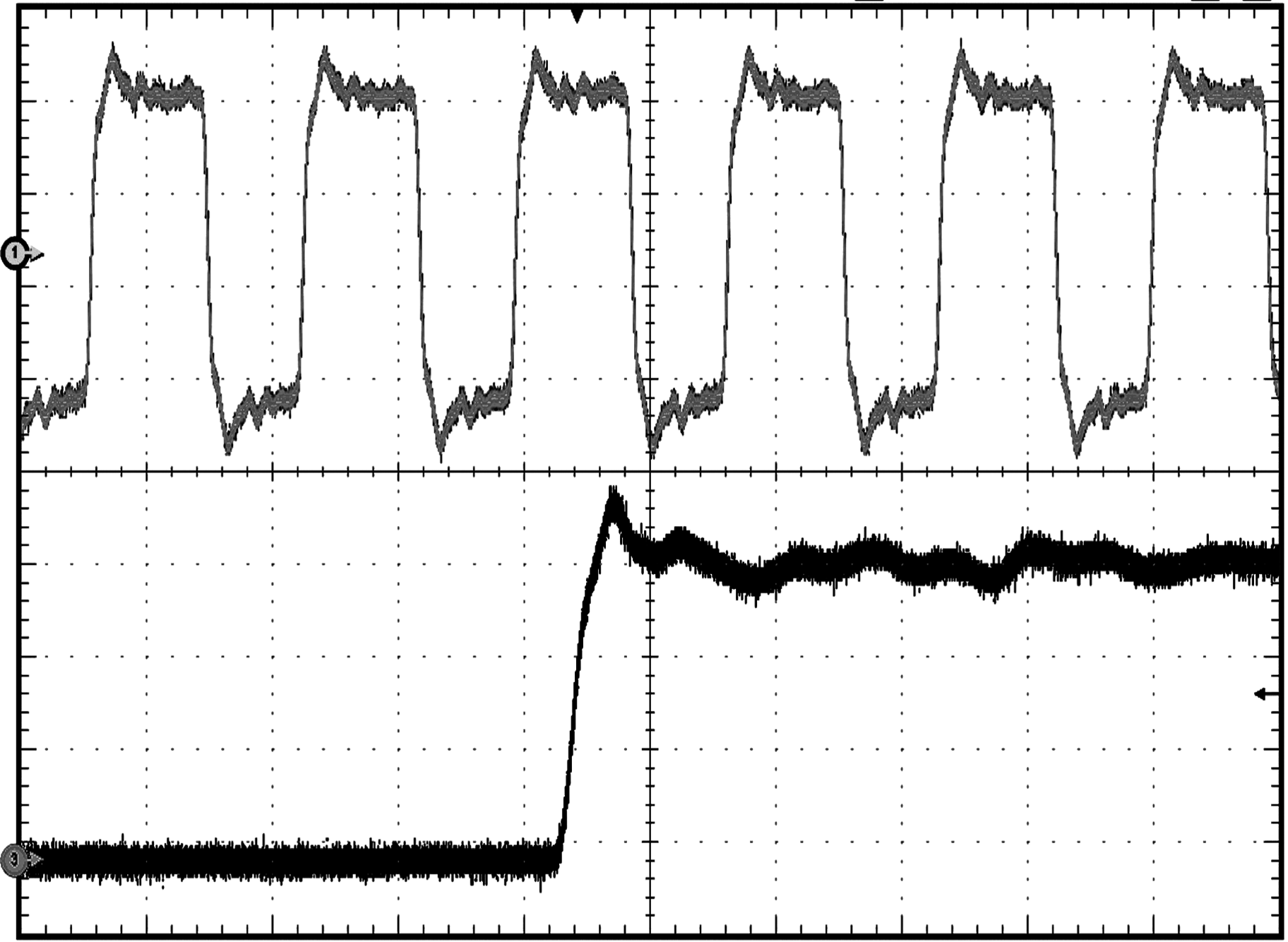
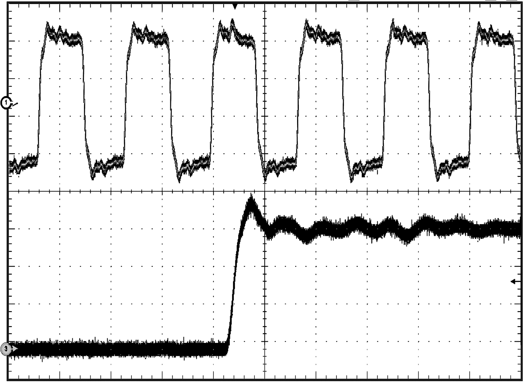
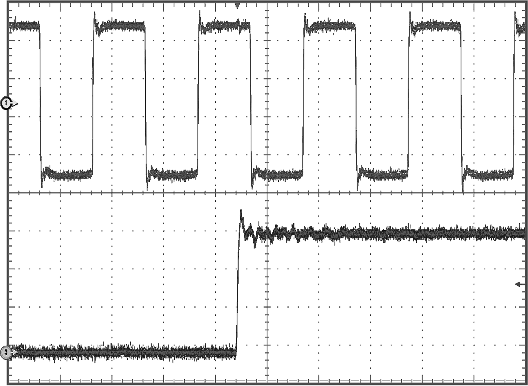
To minimize the amount of time necessary to assert lock, load LockStepSize (Register 0x2D) with a value of 0x01 and the Loss of Lock Threshold (Register 0x1C) with a value of 0x1F. The effect of this change can be seen in Figure 13:
 Figure 13. Faster NO_LOCK Reaction Mode Timing
8.3.8 LOR Determination
When the PLL is not locked, there is an internal counter that counts the number of 27 MHz clock pulses between consecutive HSync pulses divide-by-two. This counter saturates at 0x7FFF (or 32767 decimal). Once this counter saturates, LOR is declared. Given this is a divide-by-two counter, the time to declare LOR is: (2 x 32767) / (27E6) = 2.4 ms. On the other hand, when the PLL is locked and there are missing HSync pulses, LOR is set when the internal counter is greater than the following: (Number of 27 MHz clocks in one Hsync pulse + 3) x (LOR_THRES + 1).
8.3.9 Output Driver Adjustments
The LVDS output drivers can be adjusted via the I2C interface to change the differential output voltage swing, the common mode voltage, and the amount of pre-emphasis applied to the LVDS output:
- Register 0x3A, Bit 7 turns on the pre-emphasis, which may be used to extend the reach between the LMH1983 and the load. It is recommended that the trace length is kept short, as longer traces have more opportunity to couple with hostile signals and degrade jitter performance.
- The differential output swing of the CLKout pins is adjusted through Register 0x3A, Bits [6:4]. A larger value loaded into Bits [6:4] correspond to an increase in the output swing.
- The common mode output voltage can be adjusted via Register 0x3A, Bits [3:0].
8.3.10 TOF1 Alignment
Each of the four clock outputs has a corresponding Top Of Frame (TOF) output signal. The LMH1983 is programmed with a video format for each of the three video clocks (CLKout 1-3), and the TOF signal provides a digital indication when the start of a new frame occurs for that particular format. As an example, if PLL1 is programmed with a video format corresponding to NTSC, CLK1 is 27 MHz, and TOF1 outputs a pulse once per frame, or once every 900,900 clock cycles. In its default state, the LMH1983 detects the input reference format and programs this format as the output format for CLKout1. Therefore, if the input reference is an NTSC reference, then TOF1 will default to a 29.97 Hz signal.
If the HIN, VIN, and FIN inputs to the LMH1983 are coming from the LMH1981 Sync Separator, then the rising edge of the FIN input will come in the middle of a line (between HIN pulses). The TOF pulse, if aligned, will be a pulse with a width of 1 x H period and transitions aligned with the leading edges of the HIN pulses. When set for zero offset, the TOF pulse will be high during the H period where the FIN input transitions, as seen in Figure 14.
 Figure 14. TOF1 Timing
The alignment between the incoming FIN and the TOF1 output may be controlled in a number of ways. There are three different alignment modes in which TOF1 may operate as selected via Register 0x11:
- 11'b (default): PLL1 never attempts to align.
- 10'b: PLL1 always forces alignment to FIN.
- 00'b: Automatically force alignment to FIN when they are misaligned.
Once the device decides that it needs to align TOF1 and FIN, there are two ways that it can be done. Crash lock involves simply resetting the counter that keeps track of where the TOF1 output transition happens, resulting in an instantaneous shift of TOF1 to align with FIN. Drift lock involves using the second loop in PLL1 and skewing the VCXO to make the frequency of CLKout1 either speed up or slow down. The VCXO skewing slowly pulls TOF1 and FIN into alignment. If a new reference is applied that is not in alignment with TOF1, but the output is currently in use, it may be better to slew TOF1 into alignment rather than to cause a major disruption in the timing with a crash lock. The LMH1983 allows the user to select either crash lock or drift lock, controllable via Register 0x11. The option of crash lock or drift lock is available when the difference in phase is small (Output < 2LOA_window x 27 MHz Clock) and when the difference in phase is large (Output > 2LOA_window x 27 MHz Clock). Furthermore, if the difference is large, the user can tell the device to achieve alignment either by advancing or retarding the phase of PLL1. Note that if the difference in alignment is large, achieving alignment via drift lock may take a very long time (tens of seconds), during which the output clock will not be phase locked to the input HIN.
8.3.11 TOF2 and TOF3 Alignment
Similar to TOF1, CLKout2 and CLKout3 have associated video formats. The format is determined by programming Register 0x07 and 0x08, respectively. Once the format is programmed and the TOF outputs are enabled, a TOF pulse is generated at the appropriate rate for each of the outputs. There are four different alignment modes that may be selected for TOF2 and TOF3:
Table 1. TOF2/TOF3 Alignment Modes
| TOF2/TOF3 ALIGNMENT MODE | DESCRIPTION |
|---|---|
| 0 | Auto Align when Misaligned |
| 1 | One Shot Manual Align |
| 2 | Always Align |
| 3 | Never Align |
TOF2 and TOF3 are generally aligned with TOF1. The alignment status bit will only be set if the frame rates are the same as one another. Another option for alignment is via software, where the TOFX_INIT bit is set. For example, the LSB of Register 0x12 is the TOF2_INIT bit. Writing a 1 to this bit while also setting TOF2 alignment mode to anything other than 3 (Never Align) will cause TOF2 to reset its phase immediately. Note that this bit is a self-clearing bit, so it will always return a zero.
8.3.11.1 TOF3 Initialization Set Up
Under some circumstances, it is possible for an LMH1983 to power up in an anomalous state in which the output of PLL3 exhibits a large amount of cycle-to-cycle jitter. A simple register write after power up will prevent the device from remaining in this state. Writing to Register 0x13[5:4] = 10'b to force Always Align Mode ensures that the device will not exhibit poor duty cycle performance on CLKout3.
8.3.12 TOF4 Alignment
CLKout4 of the LMH1983 is most often used to generate an audio clock. The default base audio clock rate is 48 kHz, and this sample clock is synchronous in phase with the video frame only once every 5 frames for 29.97 and 30 Hz frame rate standards, or once every ten frames for 60 Hz and 59.94 Hz systems. The LMH1983 can generate a TOF4 pulse that occurs at this rate, allowing audio frames to be synchronized with the video frames.
TOF4 may be aligned either to TOF1 or to the FIN input. Additionally, there is an external INIT input that can be used to set TOF4 alignment.
| 10ns / div | ||
| Top 200mV / div | ||
| Bottom 1V / div |
Top Trace CLKout1, Bottom Trace TOF1
| 4ns / div | ||
| Top 200mV / div | ||
| Bottom 1V / div |
Top Trace CLKout3, Bottom Trace TOF3
| 4 ns / div | ||
| Top 200 mV / div | ||
| Bottom 1V / div |
Top Trace CLKout2, Bottom Trace TOF2
| 10 ns / div | ||
| Top 200 mV / div | ||
| Bottom 1V / div |
Top Trace CLKout4, Bottom Trace TOF4
8.4 Device Functional Modes
8.4.1 Reference Detection
The device uses Auto Format Detect as the default mode, as the device determines the reference format among those shown in Auto Format Detection Codes, and initiates the internal configurations accordingly. There are 31 pre-defined formats plus one format that the user can define. The device recognizes a format by measuring the HIN input frequency and looking at the VIN and FIN inputs. The device then determines if the reference input format is an interlaced or progressive input. For some formats such as a 10 MHz or 27 MHz Hsync reference, if HIN and VIN create a spurious input, the device will not properly recognize the reference input and will not lock properly to the reference. Because of this, if HIN has one of these 'special' signals on it, VIN and FIN should be muted.
8.4.2 User Defined Formats
There are several registers in the LMH1983 that are loaded automatically based on the format of the reference that is detected. The LMH1983 allows the user to define a non-standard format and a corresponding set of values to load into the appropriate registers if that format is detected. In order to identify the format, the LMH1983 measures the frequency of the Hsync input, counts the number of lines per frame in the format, and detects if the particular format is interlaced or progressive. The Hsync frequency is measured by counting the number of 27 MHz clock edges that occur in a period of time equal to 20 horizontal sync times. To implement a user defined format, the following registers are configured:
- The minimum and maximum permissible count must be set, thereby establishing a window of frequency for Hsync. Registers 0x51 and 0x52 define the 16-bit value for the low end of the frequency range, while Registers 0x53 and 0x54 define the high end of the frequency range.
- Registers 0x5A and 0x5B define the number of lines per frame for the format.
- Register 0x5D, Bit 4 indicates whether the user defined format is interlaced or not.
- Register 0x5D, Bit 7 enables the detection of a user-defined format.
- Once the user-defined format is detected, the contents of Registers 0x55 through 0x59 configure PLL1 to lock to 27MHz, which is then used as the reference for PLL2, PLL3, and PLL4.
Table 2 lists the supported standard timing formats. Table 2 includes the relevant parameters used to configure the LMH1983 for the input and output formats. Auto-detection of the input is supported for the formats listed in Table 2. The input format can also be programmed manually by the host via I2C if it is necessary to override the auto-detection feature.
Table 2. Supported Formats Lookup Table (LUT)
| FORMAT | INPUT TIMING / PLL1 PARAMETERS | OUTPUT TIMING (OUT1–4) PARAMETERS | |||||||
|---|---|---|---|---|---|---|---|---|---|
| Reference Divider | Feedback Divider | Phase Detector (PD) Freq. (kHz) | PD Periods per Frame Counter | PLL# | PLL Clock Freq. (MHz) | Total Clocks per Line Counter | Total Lines per Frame Counter | Frame Rate (Hz) |
|
| NTSC, 525i | 1 | 1716 | 15.7343 | 525 | 1 | 27.0 | 1716 | 525 | 29.97 |
| 2 | 148.5 | 9438 | |||||||
| PAL, 625i | 1 | 1728 | 15.625 | 625 | 1 | 27.0 | 1728 | 625 | 25 |
| 2 | 148.5 | 9504 | |||||||
| 525p | 1 | 858 | 31.4685 | 525 | 1 | 27.0 | 858 | 525 | 59.94 |
| 2 | 148.5 | 4719 | |||||||
| 625p | 1 | 864 | 31.25 | 625 | 1 | 27.0 | 864 | 625 | 50 |
| 2 | 148.5 | 4752 | |||||||
| 720p/60 | 1 | 600 | 45.0 | 750 | 2 | 148.5 | 3300 | 750 | 60 |
| 720p/59.94 | 5 | 3003 | 8.99101 | 150 | 3 | 148.35 | 3300 | 750 | 59.94 |
| 720p/50 | 1 | 720 | 37.5 | 750 | 2 | 148.5 | 3960 | 750 | 50 |
| 720p/30 | 1 | 1200 | 22.5 | 750 | 2 | 148.5 | 6600 | 750 | 30 |
| 720p/29.97 | 5 | 6006 | 4.49550 | 150 | 3 | 148.35 | 6600 | 750 | 29.97 |
| 720p/25 | 1 | 1440 | 18.75 | 750 | 2 | 148.5 | 7920 | 750 | 25 |
| 720p/24 | 1 | 1500 | 18.0 | 750 | 2 | 148.5 | 8250 | 750 | 24 |
| 720p/23.98 | 2 | 3003 | 8.99101 | 375 | 3 | 148.35 | 8250 | 750 | 23.98 |
| 1080p/60 | 1 | 400 | 67.5 | 1125 | 2 | 148.5 | 2200 | 1125 | 60 |
| 1080p/59.94 | 5 | 2002 | 13.48651 | 225 | 3 | 148.35 | 2200 | 1125 | 59.94 |
| 1080p/50 | 1 | 480 | 56.25 | 1125 | 2 | 148.5 | 2640 | 1125 | 50 |
| 1080p(psF)/30 | 1 | 800 | 33.75 | 1125 | 2 | 148.5 | 4400 | 1125 | 30 |
| 1080p(psF)/29.97 | 5 | 4004 | 6.74326 | 225 | 3 | 148.35 | 4400 | 1125 | 29.97 |
| 1080p(psF)/25 | 1 | 960 | 28.125 | 1125 | 2 | 148.5 | 5280 | 1125 | 25 |
| 1080p(psF)/24 | 1 | 1000 | 27.0 | 1125 | 2 | 148.5 | 5500 | 1125 | 24 |
| 1080p(psF)/23.98 | 1 | 1001 | 26.9730 | 1125 | 3 | 148.35 | 5500 | 1125 | 23.98 |
| 1080i/60 | 1 | 800 | 33.75 | 1125 | 2 | 148.5 | 4400 | 1125 | 30 |
| 1080i/59.94 | 5 | 4004 | 6.74326 | 225 | 3 | 148.35 | 4400 | 1125 | 29.97 |
| 1080i/50 | 1 | 960 | 28.125 | 1125 | 2 | 148.5 | 5280 | 1125 | 25 |
| 48 kHz word clock | 2 | 1125 | 24.0 | 1 | 4 | 98.304 | 2048 | 1 | 48000 |
| 96 kHz word clock | 4 | 1125 | 24.0 | 1 | 4 | 98.304 | 1024 | 1 | 96000 |
| 27 MHz osc clk | 1000 | 1000 | 27.000 | 1 | Input only | ||||
| 10 MHz GPS osc clk | 600 | 1620 | 16.6666 | 1 | Input only | ||||
8.4.3 Auto Format Detection Codes
The Auto Format Detection Codes apply to Registers 0x07 (Output Mode – PLL2 Format), 0x08 (Output Mode – PLL3 Format), and 0x20 (Input Format).
| FORMAT CODE | DESCRIPTION | Hsync PERIOD (in 27 MHz CLOCKS) |
INTERLACED (I) / PROGRESSIVE (P) |
|---|---|---|---|
| 0 | 525I29.97(1) | 1716 | I |
| 1 | 625I25(2) | 1728 | I |
| 2 | 525P59.94(1) | 858 | P |
| 3 | 625P50(2) | 864 | P |
| 4 | 720P60 | 600 | P |
| 5 | 720P59.94 | 600.6 | P |
| 6 | 720P50 | 720 | P |
| 7 | 720P30 | 1200 | P |
| 8 | 720P29.97 | 1201.2 | P |
| 9 | 720P25 | 1440 | P |
| 10 | 720P24 | 1500 | P |
| 11 | 720P23.98 | 1501.5 | P |
| 12 | 1080P60 | 400 | P |
| 13 | 1080P59.94 | 400.4 | P |
| 14 | 1080P50 | 480 | P |
| 15 | 1080P30 | 800 | P |
| 16 | 1080P29.97 | 800.8 | P |
| 17 | 1080P25 | 960 | P |
| 18 | 1080P24 | 1000 | P |
| 19 | 1080P23.98 | 1001 | P |
| 20 | 1080I30 | 800 | I |
| 21 | 1080I29.97 | 800.8 | I |
| 22 | 1080I25 | 960 | I |
| 23 | 1080I24 | 1000 | I |
| 24 | 1080I23.98 | 1001 | I |
| 25 | 48 kHz Audio | 562.5 | — |
| 26 | 96 kHz Audio | 281.25 | — |
| 27 | 44.1 kHz Audio | 612.244898 | — |
| 28 | 32 kHz Audio | 843.75 | — |
| 29 | 27 MHz Hsync | 1 | — |
| 30 | 10 MHz Hsync | 2.7 | — |
| 31 | User Defined | User Defined | User Defined |
| 63 | Unknown | All Others |
8.4.4 Free-Run, Genlock, and Holdover Modes
The LMH1983 primary PLL can operate in three different modes, selected via Register 0x05. These modes are Free-run, Genlock, and Holdover Mode:
- Free-run mode: HIN, VIN, and FIN are not used, and the VCXO control voltage is set by the contents of Registers 0x18 and 0x19. By writing to these registers, the VCXO voltage can be trimmed up or down. The slave PLLs will remain locked to the primary PLL.
- Genlock mode: The VCXO control voltage is actively controlled to maintain lock between HIN and the VCXO output frequency. In addition, there is a second PLL loop that may take over to assert a lock between TOF1 and FIN. See TOF1 Alignment for more details.
- Holdover mode: In the event that the reference is lost, there is an A/D — D/A pair that is able to take over for the PLL control loop and hold the VCXO control voltage constant. For this to work properly, the device must realize that it has lost its reference shortly after the reference is actually lost. Some sync separators, when the analog input is lost, will output random pulses from the H, V, and F outputs. This can confuse the device. Therefore if Holdover mode is to be used in conjunction with an analog sync separator, it is best to gate the H, V, and F signals with a signal that indicates if there is a valid reference input.
8.5 Programming
8.5.1 I2C Interface Protocol
The protocol of the I2C interface begins with the start pulse, followed by a byte which consists of a seven-bit slave device address and a Read/Write bit as an LSB. The default address of the LMH1983 for write sequences is 0xCC (11001100'b) and for read sequences is 0xCD (11001101'b). The base address can be changed with the ADDR pin. When ADDR is left open, the base address is 0x66 (which, when left shifted for a write sequence becomes 0xCC). When ADDR is connected to GND, the base address is 0x65, and when ADDR is connected to VDD, the base address is 0x67.
Please note: The I2C interface of the LMH1983 requires the 27 MHz VCXO clock input to be running in order to read I2C data packets into the 27 MHz clock domain. If the 27 MHz clock is not running, the I2C interface should still respond (ACK), but Write commands may be ignored and Read commands may return invalid data.
8.5.2 Write Sequence
The write sequence begins with a start condition, which consists of the master pulling SDA low while SCL is high. The slave address is sent next. The slave address is a seven-bit address followed by the Read/Write bit (Read = 1'b and Write = 0'b). For the default base address of 0x66 (1100110'b), the 0 is appended to the end, and the net address is 0xCC. Each byte sent after the address is followed by an ACK bit. When SCL is high, the master will release the SDA line, and the slave pulls SDA low to acknowledge. Once the device address has been sent, the next byte sent is the register address. Following the register address and the ACK, the data byte is sent. When more than one data byte is sent, the register address is automatically incremented so that the data is written into the next address location. The Write Sequence Timing Diagram is shown in Figure 19. Note that there is an ACK bit following each data byte.
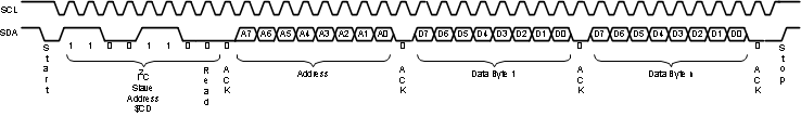 Figure 19. Write Sequence Timing Diagram
8.5.3 Read Sequence
Read sequences consist of two I2C transfers. The first is the address access transfer, which consists of a write sequence that transfers only the address to be accessed. The second is the data read transfer which starts at the address indicated in the first transfer and increments to the next address, continuing to read addresses until a stop condition is encountered. The timing diagram of the address access transfer is shown in Figure 20. A read sequence begins with a start pulse, the slave device address including the Read/Write bit (Read = 1'b and Write = 0'b), and then its ACK bit. The next byte is the address to be read, followed by the ACK bit and the stop bit to indicate the end of the address access transfer. The subsequent read data transfer shown consists of the start pulse, the slave device address including the Read/Write bit (this time a R/W Bit = 1'b, indicating that the data is to be read) and the ACK bit. The next byte is the data read from the initial access address. After each data byte is read, the address is incremented, thereby allowing the next byte of data to be read from the subsequent address of the device. Each byte is separated from the previous byte by an ACK bit, and the end of the read sequence is indicated with a STOP bit. The timing diagram for a read data transfer is shown in Figure 21 for additional timing details.
 Figure 20. Read Sequence — Address Access Transfer
 Figure 21. Read Sequence — Data Read Transfer
8.6 Register Map
The following table provides details on the device's configuration registers. Default value for fields that are seven bits or less are expressed in binary, and default values for fields that are 8 bits (Byte) are expressed in hex. Do not write to Reserved (RSVD) fields.
Table 3. LMH1983 Register Map
| ADD | NAME | BITS | FIELD | R/W | DEFAULT | DESCRIPTION |
|---|---|---|---|---|---|---|
| 0x00 | Device Status — Input Reference |
7 | INTERLACED | R | — | Indicates if the input reference format is an interlaced format |
| 6 | ANALOG_REF | R | — | This bit is set depending on if the sync detection circuit had determined if the reference is an analog or digital derived signal | ||
| 5 | INPUT_POLARITY | R | — | Returns the value of the input polarity determined by the sync detector for HSYNC — 0 indicates an active low sync | ||
| 4 | HSYNC_STATUS | R | — | This bit is set if the Hsync During Vsync detector will set NO_H_DURING_V on the next rising edge of VSYNC | ||
| 3 | H_ONLY | R | — | This is set by the Interlaced detector | ||
| 2 | LOR_STATUS | R | — | Returns the inverse of the NO_REF output pin state | ||
| 1 | LOST_HSYNC | R | — | Set if HSYNC_MISSING is high wile no_h_during_v is low. Remains set until read, then self-clears | ||
| 0 | Reserved | R | 0 | Reserved — always returns '0' | ||
| 0x01 | Device Status | 7 | Lock_Status | R | 1 | Returns lock status for all unmasked and enabled PLLs |
| 6 | Align_Status | R | 0 | Returns the Align Status for all enabled TOFs | ||
| 5 | Wrong_Format | R | 1 | Returns the value of the Wrong_Format bit. | ||
| 4 | Holdover | R | 0 | Returns the value of the PLL Holdover Bit | ||
| 3:0 | RSVD | 0000 | Reserved | |||
| 0x02 | PLL Lock and Output Alignment Status | 7:4 | Lock_Detect | R | — | [7] indicates the lock status of PLL4. [6] indicates the lock status of PLL3. [5] indicates the lock status of PLL2. [4] indicates the lock status of PLL1. 0 = PLL Not Locked 1 = PLL Locked |
| 3:0 | Align_Detect | R | — | [3] indicates the lock status of TOF4. [2] indicates the lock status of TOF3. [1] indicates the lock status of TOF2. [0] indicates the lock status of TOF1. 0 = TOF Alignment not detected 1 = TOF alignment detected |
||
| 0x03 | Revision ID | 7:0 | R | 0xC0 | Returns device revision code | |
| 0x04 | Reserved | 7:0 | RSVD | 0x00 | Reserved | |
| 0x05 | Device Control | 7 | Soft_Reset | R/W | 0 | Writing a ‘1’ will reset all registers to their default values. This bit is self-clearing and always returns ‘0’ when read. |
| 6 | Powerdown | R/W | 0 | Controls the power down function. | ||
| 5 | EN_AFD | R/W | 1 | Enables Auto Format Detection (AFD). 0 = Auto Format Detect disabled 1 = Auto Format Detect enabled |
||
| 4:3 | PLL1_Mode | R/W | 01 | Sets PLL1 operating mode: 00 = Force Free-run 01 = Genlock 10 = Force Holdover 11 = Reserved |
||
| 2 | LOR Mode | R/W | 0 | Sets default mode of operation on Loss of Reference (LOR) condition: 0 = Holdover on LOR 1 = Free-run on LOR |
||
| 1 | Force_148 | R/W | 1 | When this bit is set, it forces the PLL2 and PLL3 clock rates to 148.xx MHz regardless of chosen output format. Otherwise, the native clock rate of the chosen output format will be used. 0 = Uses the native clock rates 1 = Forces PLL2 = 148.5 MHz and PLL3 = 148.35 MHz clock rate |
||
| 0 | GOE | R/W | 1 | Global Output Enable 0 = Disables all CLKout and Fout output buffers (Hi-Z) 1 = Enable active outputs |
||
| 0x06 | Input Polarity | 7:4 | RSVD | 0000 | Reserved | |
| 3 | EN_AUTOPOL | R/W | 1 | Enables Auto Polarity Detection and Correction. The proper polarity needs to be set to synchronize the output timing signals to the leading edges of the H and V inputs. 0 = The polarities of HVF inputs are manually set by their respective polarity override registers. 1 = The polarity of the H input is auto-detected. The polarity correction applied to the H input will also be applied to V and F inputs. |
||
| 2 | HIN_POL_OVR | R/W | 0 | Used to manually set the H input Polarity. 0 = Active Low (Negative polarity) 1 = Active High (Positive polarity) |
||
| 1 | VIN_POL_OVR | R/W | 0 | Used to manually set the V input Polarity. 0 = Active Low (Negative polarity) 1 = Active High (Positive polarity) |
||
| 0 | FIN_POL_OVR | R/W | 0 | Used to manually set the F input Polarity. 0 = Active Low (Negative polarity) 1 = Active High (Positive polarity) |
||
| 0x07 | Output Mode – PLL2 Format | 7:6 | RSVD | 00 | Reserved | |
| 5:0 | PLL2_Format | R/W | 001110 | Sets the video format output timing for PLL2. | ||
| 0x08 | Output Mode – PLL3 Format | 7:6 | RSVD | 00 | Reserved | |
| 5:0 | PLL3_Format | R/W | 001101 | Sets the video format output timing for PLL3. | ||
| 0x09 | Output Mode – Misc | 7:5 | RSVD | 000 | Reserved | |
| 4 | AFS Mode | R/W | 0 | Sets the TOF4 output timing mode. 0 = Secondary Audio Clock Output (derived from PLL4 clock) 1 = Audio Frame Sync (derived from TOF1) |
||
| 3:0 | XPT_Mode | R/W | 0000 | Sets the PLL crosspoint mode for Out2 and Out3. Refer to Table 4. |
||
| 0x0A | Output Buffer Control | 7:4 | CLK_HIZ | R/W | 0000 | [3] sets CLKout4 output buffer mode. [2] sets CLKout3 output buffer mode. [1] sets CLKout2 output buffer mode. [0] sets CLKout1 output buffer mode. 0 = CLKoutx enabled 1 = CLKoutx Hi-Z |
| 3:0 | FOUT_HIZ | R/W | 1111 | [3] sets Fout4 output buffer mode. [2] sets Fout3 output buffer mode. [1] sets Fout2 output buffer mode. [0] sets Fout1 output buffer mode. 0 = Foutx enabled 1 = Foutx Hi-Z |
||
| 0x0B | Output Frame Control – Offset1_MSB | 7:5 | RSVD | 000 | Reserved | |
| 4:0 | TOF1 Offset MSB | R/W | 00000 | TOF1_Offset[12:0] sets number of lines to delay TOF1. TOF1_Offset_MSB[4:0] sets TOF1_Offset[12:8] TOF1_Offset_LSB[7:0] sets TOF1_Offset[7:0] |
||
| 0x0C | Output Frame Control – Offset1_LSB | 7:0 | TOF1 Offset LSB | R/W | 0x00 | |
| 0x0D | Output Frame Control – Offset2_MSB | 7:5 | RSVD | 000 | Reserved | |
| 4:0 | TOF2 Offset MSB | R/W | 00000 | TOF2_Offset[12:0] sets number of lines to delay TOF2. TOF2_Offset_MSB[4:0] sets TOF2_Offset[12:8] TOF2_Offset_LSB[7:0] sets TOF2_Offset[7:0] |
||
| 0x0E | Output Frame Control – Offset2_LSB | 7:0 | TOF2 Offset LSB | R/W | 0x00 | |
| 0x0F | Output Frame Control – Offset3_MSB | 7:5 | RSVD | 000 | Reserved | |
| 4:0 | TOF3 Offset MSB | R/W | 00000 | TOF3_Offset[12:0] sets number of lines to delay TOF3. TOF3_Offset_MSB[4:0] sets TOF3_Offset[12:8] TOF3_Offset_LSB[7:0] sets TOF3_Offset[7:0] |
||
| 0x10 | Output Frame Control – Offset3_LSB | 7:0 | TOF3 Offset LSB | R/W | 0x00 | |
| 0x11 | Alignment Control – TOF1 | 7:6 | RSVD | 00 | Reserved | |
| 5:4 | TOF1_Align_Mode | R/W | 11 | 00 = Auto-align when misaligned 01 = Reserved 10 = Always Align 11 = Never Align(1) |
||
| 3:2 | TOF1_Sync | R/W | 01 | This bit sets the PLL1/TOF1 output synchronization behavior when the same reference is reapplied following a momentary LOR condition and TOF1 is within 2 lines of the expected location. 00 = Always Drift Lock – ensures the outputs drift smoothly back to frame alignment without excessive output phase disturbances 01 = Drift Lock if output < (2LOA_window x 27 MHz Clock). Crash Lock otherwise. 1X = Always Crash Lock – achieves the fastest frame alignment through PLL/TOF counter resets, which can result in output phase disturbances |
||
| 1 | TOF1_Sync_Slew | R/W | 0 | Sets the direction that TOF1 slews to achieve frame alignment when a new reference is applied and TOF1 is outside of 2 lines of the expected location. 0 = TOF1 lags by railing the VCXO input low 1 = TOF1 advances by railing the VCXO input high |
||
| 0 | RSVD | 0 | Reserved | |||
| 0x12 | Alignment Control – TOF2 | 7:6 | RSVD | 00 | Reserved | |
| 5:4 | TOF2_Align_Mode | R/W | 11 | 00 = auto align when misaligned 01 = one shot manual align when writing TOF2_INIT=1 10 = always align 11 = never align |
||
| 3:1 | RSVD | 000 | Reserved | |||
| 0 | TOF2_INIT | R/W | 0 | Writing one to this bit while also writing TOF2_Align_Mode = 3, will cause the TOF2_INIT output to go high for at least one vframe period + one Hsync period and not more than one vframe period + two Hsync periods. The assertion of TOF2_INIT must happen immediately (it cannot wait for Hsync). If TOF2_Align_Mode is being written to 3, this bit will have no effect. This bit is self-clearing and will always read zero. | ||
| 0x13 | Alignment Control – TOF3 | 7:6 | RSVD | 00 | Reserved | |
| 5:4 | TOF3_Align_Mode | R/W | 11 | 00 = auto align when misaligned 01 = one shot manual align when writing TOF3_INIT=1 10 = always align 11= never align |
||
| 3:1 | RSVD | 000 | Reserved | |||
| 0 | TOF3_INIT | R/W | 0 | Writing one to this bit while also writing TOF3_Align_Mode ≠ 3, will cause the TOF3_INIT output to go high for at least one vframe period + one Hsync period and not more than one vframe period + two Hsync periods. The assertion of TOF3_init must happen immediately (it cannot wait for Hsync). If TOF3_Align_Mode is being written to 3, this bit will have no effect. This bit is self-clearing and will always read zero. | ||
| 0x14 | Alignment Control – AFS | 7:6 | RSVD | 00 | Reserved | |
| 5:4 | AFS_Align_Mode | R/W | 11 | 00 = auto align when misaligned 01 = one shot manual align. AFS_Init_Input reg determines if done by pin (INIT) or register (AFS_INIT = 1) 10 = always align 11= never align |
||
| 3 | AFS_Init_Input | R/W | 0 | 0 = Rising edges on INIT (pin 6) trigger AFS one shot manual align. 1 = Writing ‘1’ to AFS_Init register triggers AFS one shot manual align. |
||
| 2:1 | RSVD | 00 | Reserved | |||
| 0 | AFS_INIT | R/W | 0 | Writing one to this bit while also writing AFS_Align_Mode = 3 and AFS_Init_Input=1, or providing a rising edge on the init input when AFS_Align_Mode ≠ 3 and AFS_Init_Input=0, will cause the AFS_INIT output to go high for at least one vframe period + one Hsync period and not more than one vframe period + two Hsync periods. The assertion of AFS_INIT must happen immediately (it cannot wait for Hsync). If AFS_Align_Mode = 3, toggling the init input will have no effect. This bit is self-clearing and will always read zero. |
||
| 0x15 | Loss of Alignment Control | 7:3 | RSVD | 00000 | Reserved | |
| 2:0 | LOA_Window | R/W | 010 | Number of 27 MHz clocks between the TOF1 and Vsync before Loss of Alignment is reported. If the code loaded in this register is n, then Loss of Alignment will be reported if the difference between TOF1 and Vsync exceeds 2n 27 MHz clock cycles |
||
| 0x16 | LOR Control – Holdover Sampled Voltage MSB | 7:2 | RSVD | 000000 | Reserved | |
| 1:0 | VC_Hold_MSB | R | 10 | The VC_Hold[9:0] input signal changes rather slowly. For synchronization, it should be sampled on consecutive 27 MHz clocks until two identical values are found. This value will be saved as VC_Hold_sampled[9:0]. Whenever the VC_Hold[9:8] register is read, VC_Hold_sampled[9:8] is returned, and VC_Hold[7:0] will memorize the current value of VC_Hold_sampled[7:0] (to be read at a later time). This scheme allows a coherent 10-bit value to be read. Returns a synchronized snapshot of the VC_Hold[9:8] (MSB). |
||
| 0x17 | LOR Control – Holdover Sampled Voltage LSB | 7:0 | VC_Hold_LSB | R | — | The VC_Hold[9:0] input signal changes rather slowly. For synchronization, it should be sampled on consecutive 27 MHz clocks until two identical values are found. This value will be saved as VC_Hold_sampled[9:0]. Whenever the VC_Hold[9:8] register is read, VC_Hold_sampled[9:8] is returned, and VC_Hold[7:0] will memorize the current value of VC_Hold_sampled[7:0] (to be read at a later time). This scheme allows a coherent 10-bit value to be read. Returns a synchronized snapshot of the VC_Hold[7:0] (LSB) |
| 0x18 | LOR Control Free-run Control Voltage MSB | 7:2 | RSVD | Reserved | ||
| 1:0 | VC_Free_MSB | R/W | 01 | Free-run Control Voltage (VC_Free[9:0]) is the voltage asserted on VC_LPF pin in free-run mode. Writing will change the MSB (VC_Free[9:8]) |
||
| 0x19 | LOR Control – Free-run Control Voltage LSB | 7:0 | VC_Free_LSB | R/W | 0xFF | Free-run Control Voltage (VC_Free[9:0]) is the voltage asserted on VC_LPF pin in free-run mode. Writing will change the LSB (VC_Free[7:0]) |
| 0x1A | LOR Control – ADC and DAC Disable | 7:2 | RSVD | 000000 | Reserved | |
| 1 | ADC_Disable | R/W | 0 | Directly controls the ADC_Disable output port. 0 = enable holdover ADC 1 = disable holdover ADC |
||
| 0 | DAC_Disable | R/W | 0 | Directly controls the DAC_Disable output port. 0 = enable Free-run/Holdover DAC 1 = disable Free-run/Holdover DAC |
||
| 0x1B | Loss of Reference Threshold | 7 | RSVD | 0 | Reserved | |
| 6:4 | HSYNC_Missing Threshold | R/W | 00 | Sets the threshold for number of additional clocks to wait before setting HSYNC_Missing. | ||
| 3 | RSVD | 0 | Reserved | |||
| 2:0 | LOR_Threshold | R/W | 001 | Sets the number of Hsync periods to wait before setting loss of reference. Since during blanking there can have up to 5 missing Hsync pulses, this value is usually set to 6. | ||
| 0x1C | Loss of Lock Threshold | 7:5 | RSVD | 000 | Reserved | |
| 4:0 | LOCK1_Threshold | R/W | 10000 | Sets the number of Hsync periods to wait before setting loss of lock. Since during blanking there can have up to 5 missing Hsync pulses, this value is usually set > 6. | ||
| 0x1D | Mask Control – PLL Lock and Output Align | 7 | MASK_LOCK4 | R/W | 0 | Setting this bit masks the PLL4 lock status in the global LOCK_STATUS bit. |
| 6 | MASK_LOCK3 | R/W | 0 | Setting this bit masks the PLL3 lock status in the global LOCK_STATUS bit. | ||
| 5 | MASK_LOCK2 | R/W | 0 | Setting this bit masks the PLL2 lock status in the global LOCK_STATUS bit. | ||
| 4 | MASK_LOCK1 | R/W | 0 | Setting this bit masks the PLL1 lock status in the global LOCK_STATUS bit. | ||
| 3 | MASK_TOF4_ALIGN | R/W | 0 | Setting this bit masks the TOF4 align status in the global ALIGN_STATUS bit. | ||
| 2 | MASK_TOF3_ALIGN | R/W | 0 | Setting this bit masks the TOF3 align status in the global ALIGN_STATUS bit. | ||
| 1 | MASK_TOF2_ALIGN | R/W | 0 | Setting this bit masks the TOF2 align status in the global ALIGN_STATUS bit. | ||
| 0 | MASK_TOF1_ALIGN | R/W | 0 | Setting this bit masks the TOF1 align status in the global ALIGN_STATUS bit. | ||
| 0x1E | Reserved | 7:0 | RSVD | 0x00 | Reserved | |
| 0x1F | Reserved | 7:0 | RSVD | 0x00 | Reserved | |
| 0x20 | Input Format | 7:6 | RSVD | 00 | Reserved | |
| 5:0 | Input Format | 000000 | When Auto Format Detection is enabled (EN_AFD, address 0x05), this register is read-only and controlled automatically. When Auto Format Detection is disabled, this register is writable via I2C. All writes to this register (whether automatic or manual) will update all the LUT1 (Lookup Table 1), LUT2_2, and LUT2_3 output registers based on the value written here. Writing to any of the LUT1, LUT2_2, or LUT2_3 output registers will set this field to 6’d62 (0x3E) indicating that custom changes have been made. |
|||
| 0x21 | Output Frame Lookup – Input Vsync Code | 7:4 | RSVD | 00 | Reserved | |
| 3:0 | Input Vsync Code | R/W | 0011 | Writes to this register update the Vsync code which tells the device what the Input frame rate is. There is a table which correlates the Vsync codes to the actual frame rates. When Auto Format Detection is enabled (EN_AFD, address 5), this register is read-only, and is automatically loaded by the device. | ||
| 0x22 | Output Frame Lookup – PLL2 Vsync Code | 7:4 | RSVD | 00 | Reserved | |
| 3:0 | PLL2 Vsync Code | R/W | 0101 | Whenever PLL2_FORMAT (address 7) is written, this field is updated with the appropriate Vsync code. If any custom changes are made the device will set this field to 4’d14 (0x0E) to so indicate. | ||
| 0x23 | Output Frame Lookup – PLL3 Vsync Code | 7:4 | RSVD | 0000 | Reserved | |
| 3:0 | PLL3 Vsync Code | R/W | 0110 | Whenever PLL3_FORMAT (address 8) is written, this field is updated with the appropriate Vsync code. If any custom changes are made the device will set this field to 4’d14 (Ox0E) to so indicate. | ||
| 0x24 | Reserved | 7:0 | RSVD | 0x00 | Reserved | |
| 0x25 | PLL1 Advanced Control | 7:5 | RSVD | 000 | Reserved | |
| 4 | PLL1_DIV | R/W | 0 | 0 = Divide by 1 (Output is 27 MHz) 1 = Divide by 2 (Output is 13.5 MHz) |
||
| 3 | RSVD | 0 | Reserved | |||
| 2 | PLL1 Input Mode | R/W | 0 | Directly controls the mode of the PLL1 input buffer. 0 = Single Ended 1 = Differential |
||
| 1 | RSVD | 0 | Reserved | |||
| 0 | FastLock | 1 | This bit enables ICP1_FAST (address 0x27) to be used during locking. 0 = FastLock disabled 1 = FastLock enabled |
|||
| 0x26 | PLL1 Advanced Control FastLock Delay | 7:4 | RSVD | 0000 | Reserved | |
| 3:0 | FastLock Delay | R/W | 0000 | Sets the amount of time that PLL1_Lock must be asserted before the PLL1 Charge pump current is reduced from the ICP1_Fast value to the ICP1 value. The time delay is specified in units of half seconds. Delay = FastlockDelay*0.5 Seconds. Valid values are from 0 to 10. Values from 11 to 15 are reserved. | ||
| 0x27 | PLL1 Advanced Control Fastlock CP Current |
4:0 | FastLock Charge Pump Current | R/W | 11111 | This field specifies the charge pump current to drive when FastLock is active. Charge pump current is equal to 34.375 µA * register value |
| 0x28 | PLL1 Advanced Control Charge Pump Current |
4:0 | PLL1 Charge Pump Current | R/W | 01000 | This field defines the charge pump current used when FastLock is not active. Charge pump current is equal to 34.375 µA * register value |
| 0x29 | PLL1 Advanced Control R Counter MSB |
7:2 | RSVD | 000000 | Reserved | |
| 1:0 | MSB | R/W | 00 | The two LSBs of Register 0x29 along with the eight bits of Register 0x2A form a ten bit word which comprises the R divider for PLL1. This register is internally written based on the input format and when AutoFormatDetect is enabled, these registers are read only. | ||
| 0x2A | PLL1 Advanced Control R Counter LSB |
7:0 | LSB | R/W | 0x01 | |
| 0x2B | PLL1 Advanced Control N Counter MSB |
7 | RSVD | 0 | Reserved | |
| 6:0 | MSB | R/W | 0000110 | The 7 LSBs of Register 0x2B along with the eight bits of Register 0x2C comprise the fifteen bit word which is used for the N divider of PLL1. These registers are internally controlled based on the input format detected and when AutoFormatDetect is enabled, these registers are read only. | ||
| 0x2C | PLL1 Advanced Control N Counter LSB |
7:0 | LSB | R/W | 0xB4 | |
| 0x2D | PLL1 Advanced Control Lock Step Size |
7:5 | RSVD | 000 | Reserved | |
| 4:0 | Lock Step Size | R/W | 01000 | See Application Information section discussion on Lock Detect | ||
| 0x2E | PLL2 Advanced Control Main |
7:5 | RSVD | 000 | Reserved | |
| 4 | PLL2_DIV | R/W | 0 | 0 = divide by 1 1 = divide by 2 |
||
| 3 | PLL2_DISABLE | R/W | 0 | 0 = PLL2 disable is determined by XPT_MODE (Address 0x09) 1 = PLL2 is disabled |
||
| 2:0 | RSVD | 000 | Reserved | |||
| 0x2F | PLL2 Advanced Control Charge Pump Current |
7:4 | RSVD | 0000 | Reserved | |
| 3:0 | ICP2 | R/W | 0010 | Controls PLL2 Charge Pump Current | ||
| 0x30 | PLL2 Advanced Control VCO Range |
7:0 | VCO_RNG2 | R/W | 0x0C | Controls the VCO range |
| 0x31 | PLL3 Advanced Control Main |
7:5 | RSVD | 000 | Reserved | |
| 4 | PLL3_DIV | R/W | 0 | 0 = divide by 1 1 = divide by 2 |
||
| 3 | ICP3 | R/W | 0 | 0 = PLL3 disable is determined by XPT_MODE (Address 0x09) 1 = PLL3 is disabled |
||
| 2:0 | RSVD | 000 | Reserved | |||
| 0x32 | PLL3 Advanced Control Charge Pump Current |
7:4 | RSVD | 0000 | Reserved | |
| 3:0 | ICP3 | R/W | 0011 | Controls PLL3 Charge Pump Current | ||
| 0x33 | PLL3 Advanced Control VCO Range |
7:0 | VCO_RNG3 | R/W | 0x05 | Controls the VCO range |
| 0x34 | PLL4 Advanced Control Main |
7:4 | PLL4_DIV | R/W | 0010 | Controls the PLL4 output divider — PLL4 is divided by 2PLL4_DIV |
| 3 | PLL4_Disable | R/W | 0 | 0 = PLL4 is enabled 1 = PLL4 is disabled |
||
| 2 | RSVD | 0 | Reserved | |||
| 1 | IS125M | R/W | 0 | 0 = 100 MHz clock 1 = 125 MHz clock |
||
| 0 | PLL4_Mode | R/W | 0 | 0 = using 27 MHz Clock 1 = using external clock |
||
| 0x35 | PLL4 Advanced Control Charge Pump Current |
7:4 | RSVD | 0000 | Reserved | |
| 3:0 | ICP4 | R/W | 1000 | Controls PLL4 Charge Pump Current | ||
| 0x36 | PLL4 Advanced Control R counter |
7 | RSVD | 0 | Reserved | |
| 6:0 | DIV_R4 | R/W | 1001011 | Sets the R divider in PLL4 | ||
| 0x37 | PLL4 Advanced Control N counter MSB |
7:2 | RSVD | 000000 | Reserved | |
| 1:0 | DIV_N4_MSB | R/W | 10 | Two MSBs of the N divider in PLL4 | ||
| 0x38 | PLL4 Advanced Control N counter LSB |
7:0 | DIV_N4_LSB | R/W | 0x00 | 8 LSBs of the N divider in PLL4 |
| 0x39 | PLL4 Advanced Control VCO Range |
7:0 | VCO4 Range | R/W | 0x16 | The value in the VCO4 Range register is used to adjust the center frequency of PLL4. |
| 0x3A | LVDS Control | 7 | LVDS Boost | R/W | 0 | Applies pre-emphasis to LVDS output |
| 6:4 | LVDS_DIFF | R/W | 100 | Adjusts LVDS Differential output swing | ||
| 3:0 | LVDS_CM | R/W | 1001 | Adjusts LVDS Common Mode output voltage | ||
| 0x3B | TOF1 Adv Control LPF MSB |
7:5 | RSVD | 000 | Reserved | |
| 4:0 | TOF1_LPF_MSB | R | 00010 | 5 MSBs of the TOF1 lines per Frame count. This is read-only and loaded automatically when Auto Format Detection is enabled | ||
| 0x3C | TOF1 Advanced Control LPF_LSB |
7:0 | TOF1_LPF_LSB | R | 0x0D | 8 LSBs of the TOF1 lines per Frame count. This is read-only and loaded automatically when Auto Format Detection is enabled Together with Register 0x3B this is a 13 bit number which number of lines per frame. TOF1 will be at a frequency of Hsync divided by this value. |
| 0x3D | TOF2 Advanced Control CPL MSB |
7 | RSVD | 0 | Reserved | |
| 6:0 | TOF2_CPL_MSB | R | 0001010 | This 15 bit register gives the number of clock cycles per line to calculate TOF2. It is loaded automatically based on the format set with Register 0x07. | ||
| 0x3E | TOF2 Advanced Control CPL LSB |
7:0 | TOF2_CPL_LSB | R | 0x50 | |
| 0x3F | TOF2 Advanced Control LPF MSB |
7:5 | RSVD | 000 | Reserved | |
| 4:0 | TOF2_LPF_MSB | R | 00010 | This 13 bit register is loaded automatically based on the format selected via Register 0x07. It sets the number of lines per frame for the selected format to set the TOF2 rate correctly. | ||
| 0x40 | TOF2 Advanced Control LPF_LSB |
7:0 | TOF2_LPF_LSB | R | 0x65 | |
| 0x41 | TOF2 Advanced Control Frame Reset MSB |
7:5 | RSVD | 000 | Reserved | |
| 4:0 | TOF2_RST_MSB | R | 00010 | Automatically loaded based on formats selected. | ||
| 0x42 | TOF2 Advanced Control Frame Reset LSB |
7:0 | TOF2_RST_LSB | R | 0x58 | |
| 0x43 | TOF3 Advanced Control CPL_MSB |
7 | RSVD | 0 | Reserved | |
| 6:0 | TOF3_CPL_MSB | R | 0001000 | This 15 bit register gives the number of clock cycles per line to calculate TOF3. It is loaded automatically based on the format set with Register 0x08. | ||
| 0x44 | TOF3 Advanced Control CPL_LSB |
7:0 | TOF2_CPL_LSB | R | 0x98 | |
| 0x45 | TOF3 Advanced Control LPF_MSB |
7:5 | RSVD | 000 | Reserved | |
| 4:0 | TOF3_LPF_MSB | R | 00100 | This 13 bit register is loaded automatically based on the format selected via Register 0x08. It sets the number of lines per frame for the selected format to set the TOF3 rate correctly. | ||
| 0x46 | TOF3 Advanced Control LPF_LSB |
7:0 | TOF3_LPF_LSB | R | 0x65 | |
| 0x47 | TOF3 Advanced Control Frame Reset MSB |
7:5 | RSVD | 000 | Reserved | |
| 4:0 | TOF3_RST_MSB | R | 00000 | Automatically loaded based on formats selected. | ||
| 0x48 | TOF3 Advanced Control Frame Reset LSB |
7:0 | TOF3_RST_LSB | R | 0x01 | |
| 0x49 | TOF4 Advanced Control AFS |
7:0 | TOF4_AFS | R/W | 0x05 | See Detailed Description section for details. See also PLL4 Block Diagram. |
| 0x4A | TOF4 Advanced Control ACLK |
7:4 | RSVD | 0000 | Reserved | |
| 3:0 | TOF4_ACLK | R/W | 1011 | See Detailed Description section for details. See also PLL4 Block Diagram. | ||
| 0x4B to 0x50 |
Reserved | 7:0 | RSVD | 0x00 | Reserved | |
| 0x51 | User Auto Format 27M High Value MSB |
7:0 | USR_27M_High_MSB | R/W | 0x00 | User format detect is determined by looking at the frequency of the Hsync input. This frequency is measured by counting the number of 27 MHz clock cycles that occur in 20 Hsync periods. This 16 bit register lists the maximum number of 27 MHz clock cycles in 20 Hsync periods that could be considered to meet the criteria for the User Format |
| 0x52 | User Auto Format 27M High Value LSB |
7:0 | USR_27M_High_LSB | R/W | 0x00 | |
| 0x53 | User Auto Format 27M Low Value MSB |
7:0 | USR_27M_Low_MSB | R/W | 0x00 | User format detect is determined by looking at the frequency of the Hysnc input. This frequency is measured by counting the number of 27 MHz clock cycles that occur in 20 Hsync periods. This 16 bit register lists the minimum number of 27 MHz clock cycles in 20 Hsync periods that could be considered to meet the criteria for the User Format |
| 0x54 | User Auto Format 27M Low Value LSB |
7:0 | USR_27M_Low_LSB | R/W | 0x00 | |
| 0x55 | User Auto Format R divider MSB |
7:2 | RSVD | 000000 | Reserved | |
| 1:0 | USR_DIV_R1_MSB | R/W | 00 | See Detailed Description section for details. | ||
| 0x56 | User Auto Format R Divider LSB |
7:0 | USR_DIV_R1_LSB | R/W | 0x00 | See Detailed Description section for details. |
| 0x57 | User Auto Format N Divider MSB |
7 | RSVD | 0 | Reserved | |
| 6:0 | USR_DIV_N1_MSB | R/W | 0000000 | See Detailed Description section for details. | ||
| 0x58 | User Auto Format N Divider LSB |
7:0 | USR_DIV_N1_LSB | R/W | 0x00 | See Detailed Descriptionsection for details. |
| 0x59 | User Auto Format Charge Pump Current |
7:0 | USR_ICP | R/W | 0x00 | See Detailed Description section for details. |
| 0x5A | User Auto Format LPF MSB |
7:5 | RSVD | 000 | Reserved | |
| 4:0 | USR_TOF_LPF_MSB | R/W | 00000 | See Detailed Description section for details. | ||
| 0x5B | User Auto Format LPF LSB |
7:0 | USR_TOF_LPF_MSB | R/W | 0x00 | See Detailed Description section for details. |
| 0x5C | User Auto Format AFS |
7:0 | USR_TOF4 | R/W | 0x00 | See Detailed Description section for details. |
| 0x5D | User Auto Format Misc |
7 | EN_USERMODE | R/W | 0 | Enables the Auto Format Detection User Mode. 0 = disabled 1 = enabled |
| 6:5 | RSVD | 00 | Reserved | |||
| 4 | USR_IINTERLACED | R/W | 0 | Sets the INTERLACED value to output from LUT1 if the INPUT_FORMAT register is set to the user code. This bit also specifies the value that the Auto Format Detection must see on the interlaced signal to detect the user defined mode. | ||
| 3:0 | USR_IN_VS_CODE | R/W | 0000 | Sets the INPUT_VS_CODE value to output from LUT1 if the INPUT_FORMAT registers is set to the user code. |
Table 4. Crosspoint Output Selection Table
| REGISTER 0x09 [3:0] | PLL2_DISABLE(1) | PLL3_DISABLE(1) | OUT2 SOURCE | OUT3 SOURCE |
|---|---|---|---|---|
| 0000 (default) | 0 | 0 | PLL2 | PLL3 |
| 0001 | 1 | 1 | PLL1 | PLL1 |
| 0010 | 0 | 1 | PLL2 | PLL2 |
| 0011 | 1 | 0 | PLL3 | PLL3 |
| 0100 | 0 | 0 | PLL3 | PLL2 |
| 0101 | 1 | 0 | PLL1 | PLL3 |
| 0110 | 0 | 1 | PLL2 | PLL1 |
| 0111 | 0 | 1 | PLL1 | PLL2 |
| 1000 | 1 | 0 | PLL3 | PLL1 |
| 1001 | Reserved | Reserved | Reserved | Reserved |
| 1010 | Reserved | Reserved | Reserved | Reserved |
| 1011 | Reserved | Reserved | Reserved | Reserved |
| 1100 | Reserved | Reserved | Reserved | Reserved |
| 1101 | Reserved | Reserved | Reserved | Reserved |
| 1110 | Reserved | Reserved | Reserved | Reserved |
| 1111 | Reserved | Reserved | Reserved | Reserved |
Table 5. Vsync Codes
| Vsync CODE NUMBER (BINARY)(1) |
FRAME RATE (Hz) |
|---|---|
| 0 (0000) | 23.98 Hz |
| 1 (0001) | 24 Hz |
| 2 (0010) | 25 Hz |
| 3 (0011) | 29.97 Hz |
| 4 (0100) | 30 Hz |
| 5 (0101) | 50 Hz |
| 6 (0110) | 59.94 Hz |
| 7 (0111) | 60 Hz |