SNLS309I April 2010 – December 2014 LMH1983
PRODUCTION DATA.
- 1 Features
- 2 Applications
- 3 Description
- 4 Revision History
- 5 Description (continued)
- 6 Pin Configurations and Functions
- 7 Specifications
-
8 Detailed Description
- 8.1 Overview
- 8.2 Functional Block Diagram
- 8.3
Feature Description
- 8.3.1 Control of PLL1
- 8.3.2 PLL1 Loop Response Design Equations
- 8.3.3 Control of PLL2 and PLL3
- 8.3.4 Control of PLL4
- 8.3.5 Clock Output Jitter
- 8.3.6 Lock Determination
- 8.3.7 Lock Time Considerations
- 8.3.8 LOR Determination
- 8.3.9 Output Driver Adjustments
- 8.3.10 TOF1 Alignment
- 8.3.11 TOF2 and TOF3 Alignment
- 8.3.12 TOF4 Alignment
- 8.4 Device Functional Modes
- 8.5 Programming
- 8.6 Register Map
- 9 Applications and Implementation
- 10Power Supply Recommendations
- 11Layout
- 12Device and Documentation Support
- 13Mechanical, Packaging, and Orderable Information
Package Options
Mechanical Data (Package|Pins)
- RTA|40
Thermal pad, mechanical data (Package|Pins)
- RTA|40
Orderable Information
7 Specifications
7.1 Absolute Maximum Ratings
over operating free-air temperature range (unless otherwise noted) (1)(3)(2)| MIN | MAX | UNIT | |||
|---|---|---|---|---|---|
| VDD | Supply voltage | 3.6 | V | ||
| VI | Input voltage (any input) | -0.3 | VDD + 0.3 | V | |
| VO | Output voltage (any output) | -0.3 | VDD + 0.3 | V | |
| TJMAX | Junction temperature | 150 | °C | ||
| Tstg | Storage temperature range | -65 | 150 | °C | |
(1) Absolute Maximum Ratings are limits beyond which damage to the device may occur. Operating Ratings are conditions under which operation of the device is intended to be functional. For ensured specifications and test conditions, see the Electrical Characteristics. Stresses beyond those listed under Absolute Maximum Ratings may cause permanent damage to the device. These are stress ratings only, which do not imply functional operation of the device at these or any other conditions beyond those indicated under Recommended Operating Conditions. Exposure to absolute-maximum-rated conditions for extended periods may affect device reliability.
(2) If Military/Aerospace specified devices are required, please contact the Texas Instruments Sales Office/ Distributors for availability and specifications.
(3) For soldering information, see SNOA549.
7.2 ESD Ratings
| VALUE | UNIT | |||
|---|---|---|---|---|
| V(ESD) | Electrostatic discharge | Human-body model (HBM), per ANSI/ESDA/JEDEC JS-001(1) | 2500 | V |
| Machine model (MM)(3) | 250 | |||
| Charged-device model (CDM), per JEDEC specification JESD22-C101(2) | 750 | |||
(1) JEDEC document JEP155 states that 500-V HBM allows safe manufacturing with a standard ESD control process. Manufacturing with less than 500-V HBM is possible with the necessary precautions. Pins listed as ±2500 V may actually have higher performance.
(2) JEDEC document JEP157 states that 250-V CDM allows safe manufacturing with a standard ESD control process. Manufacturing with less than 250-V CDM is possible with the necessary precautions. Pins listed as ±750 V may actually have higher performance.
(3) Machine Model, applicable std. JESD22-A115-A (ESD MM std. of JEDEC).
7.3 Recommended Operating Conditions
over operating free-air temperature range (unless otherwise noted)| MIN | NOM | MAX | UNIT | ||
|---|---|---|---|---|---|
| Input Voltage | 0 | VDD | V | ||
| Temperature Range, TA | -40 | 85 | °C | ||
7.4 Thermal Information
| THERMAL METRIC(1) | RTA | UNIT | |
|---|---|---|---|
| 40 PINS | |||
| TJMAX | Junction Temperature, VDD | 3.3 ± 5% | °C/W |
| RθJA | Thermal Resistance(2) | 33 | °C/W |
(1) For more information about traditional and new thermal metrics, see the IC Package Thermal Metrics application report, SPRA953.
(2) The maximum power dissipation is a function of TJ(MAX), RθJA. The maximum allowable power dissipation at any ambient temperature is PD = (TJ(MAX) – TA)/ RθJA. All numbers apply for packages soldered directly onto a PC Board.
7.5 Electrical Characteristics(1)
Unless otherwise specified, all limits are specified for TA = 25°C, VDD = 3.3 V, RL_CLK = 100 Ω (CLKout differential load).| PARAMETER | TEST CONDITIONS | MIN(3) | TYP(2) | MAX(3) | UNIT | |
|---|---|---|---|---|---|---|
| IDD | Total supply current | Default register settings, no load on logic outputs. VDD = 3.465 V | 170 | 212 | mA | |
| IDD | Total supply current | PLL2, PLL3 and PLL4 disabled, no load on logic outputs. VDD = 3.465 V | 60 | 100 | mA | |
| REFERENCE INPUTS (Hin, Vin, Fin) | ||||||
| VIL | Low input voltage | IIN = ±10 μA | 0 | 0.3 VDD | V | |
| VIH | High input voltage | IIN = ±10 µA | 0.7 VDD | VDD | V | |
| TAFD | Auto-format detection time | Time from when reference input first presented to when detected as indicated by NO_REF going low. Reference timing must be stable and accurate (no missing pulses). | 2 | 4 | Input Frames | |
| OSCin LOGIC INPUTS | ||||||
| VIL | Low input voltage | IIN = ±10 µA | 0 | 0.3 VDD | V | |
| VIH | High input voltage | IIN = ±10 µA | 0.7 VDD | VDD | V | |
| I2C INTERFACE (SDA, SCL) | ||||||
| VIL | Low input voltage | 0 | 0.3 VDD | V | ||
| VIH | High input voltage | 0.7 VDD | VDD | V | ||
| IIN | Input current | VIN between 0.1 VDD and 0.9 VDD | −10 | +10 | μA | |
| IOL | Low output sink current | VOL = 0V or 0.4V | 1.25 | mA | ||
| STATUS FLAG OUTPUTS (NO_REF, NO_ALIGN,NO_LOCK) | ||||||
| VOL | Low output voltage | IOUT = +10 mA | 0.4 | V | ||
| VOH | High output voltage | IOUT = −10 mA | VDD-0.4V | V | ||
| FRAME TIMING OUTPUTS | ||||||
| VOL | Low output voltage | IOUT = +10 mA Fout1, Fout2, Fout3(6) |
0.4 | |||
| VOH | High output voltage | IOUT = -10mA Fout1, Fout2, Fout3(6) |
VDD-0.4 V | |||
| IOZ | Output shutdown leakage current | Output buffer shutdown, pin connected to VDD or GND VDD = 3.465V | 0.4 | 10 | |μA| | |
| VIDEO and AUDIO CLOCK OUTPUTS (CLKout1, CLKout2 and CLKout3) | ||||||
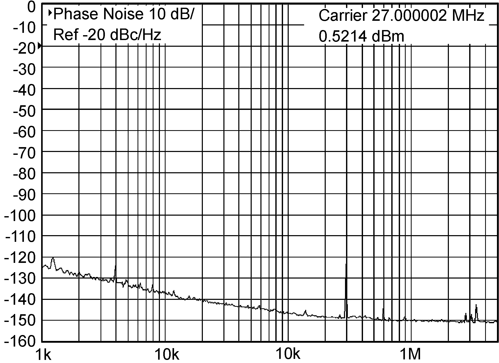
| tDJ | 27 MHz TIE deterministic Jitter | Measured at CLKout1 all other CLKouts shutdown | 250 | fs | ||
| Measured at CLKout1, other CLKouts output default PLL | 250 | fs | ||||
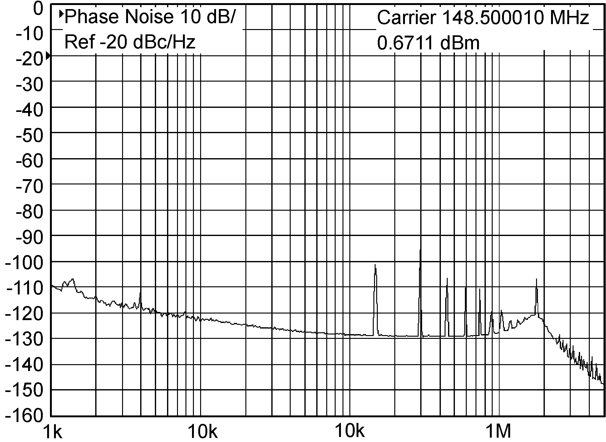
| 148.5 MHz TIE deterministic Jitter | Measured at CLKout2 all other CLKouts shutdown | 8 | ps | |||
| Measured at CLKout2, other CLKouts output default PLL | 8 | ps | ||||
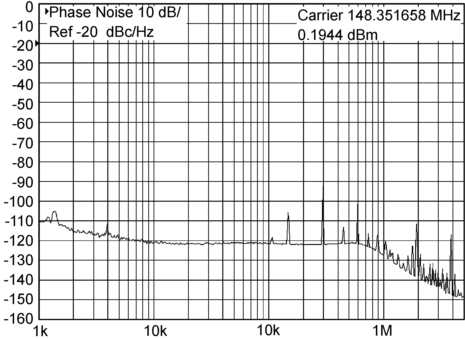
| 148.35 MHz TIE deterministic Jitter | Measured at CLKout3 all other CLKouts shutdown | 4 | ps | |||
| Measured at CLKout3, other CLKouts output default PLL | 4 | ps | ||||
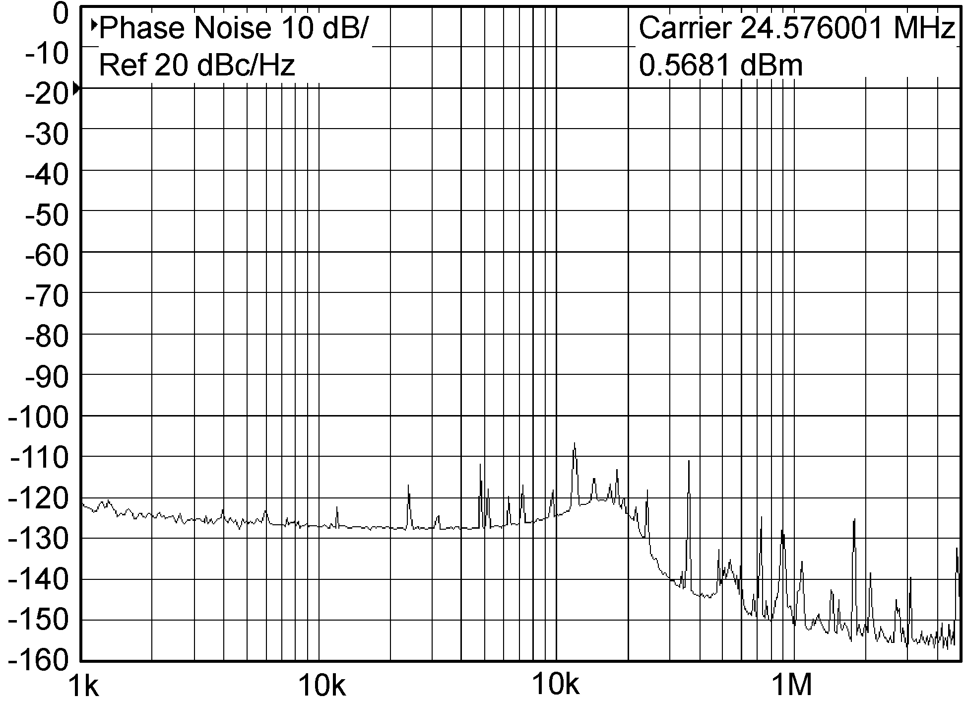
| 24.576 MHz TIE deterministic Jitter | Measured at CLKout4 all other CLKouts shutdown | 15 | ps | |||
| Measured at CLKout4, other CLKouts output default PLL | 15 | ps | ||||
| tRJ | 27 MHz TIE random Output Jitter(4) | Measured at CLKout1, other CLKouts shutdown | 2.7 | ps | ||
| Measured at CLKout1, other CLKouts output default PLL | 2.7 | ps | ||||
| 148.5 MHz TIE Random Output Jitter(4) | Measured at CLKout2, other CLKouts shutdown | 3.0 | ps | |||
| Measured at CLKout2, other CLKouts output default PLL | 3.0 | ps | ||||
| 148.35 MHz TIE Random Output Jitter (4) | Measured at CLKout3, other CLKouts shutdown | 3.5 | ps | |||
| Measured at CLKout3, other CLKouts output default PLL | 3.5 | ps | ||||
| 24.576 MHz TIE Random Output Jitter(4) | Measured at CLKout4, other CLKouts shutdown | 3.4 | ps | |||
| Measured at CLKout4, other CLKouts output default PLL | 3.4 | ps | ||||
| TD | Duty cycle | Measured at 50% level of clock amplitude, any output clock | 50% | |||
| tR | Rise time 20% to 80% |
15 pF load | 400 | ps | ||
| tF | Fall time 80% to 20% |
15 pF load | 400 | ps | ||
| VOD | Differential signal output voltage | 100 Ω differential load, CLKout1, CLKout2 or CLKout3(7) | 247 | 350 | 454 | mV |
| VOS | Common signal output voltage | 100 Ω differential load, CLKout1, CLKout2 or CLKout3(7) | 1.125 | 1.25 | 1.375 | V |
| |VOD| | |Change to VOD| for complementary output states | 100 Ω differential load, CLKout1, CLKout2 or CLKout3(7) | 50 | |mV| | ||
| |VOS| | |Change to VOS| for complementary output states | 100 Ω differential load, CLKout1, CLKout2 or CLKout3(7) | 50 | |mV| | ||
| IOS | Output short circuit current | Differential clock output pins connected to GND for CLKout1, CLKout2, or CLKout3 | 24 | |mA| | ||
| IOZ | Output shutdown leakage current | Output buffer in shutdown mode, differential clock output pins connected to VDD or GND | 1 | 10 | |µA| | |
| VCXO INPUT (XOin) | ||||||
| fOFF | Maximum relative frequency offset between VCXO input and H input | Assumes H input jitter of ±15 ns | ±150 | ppm | ||
| VXOin_SE | Single-ended signal input voltage range | Single-ended input buffer mode | 0 | VDD | V | |
| VXOin_DIFF | Differential signal input voltage range | Differential input buffer mode, VCM = 1.2 V | 247 | 350 | 454 | mV |
| DIGITAL HOLDOVER and FREE-RUN SPECIFICATIONS | ||||||
| VVCout_RNG | DAC output voltage range | Digital Free-run Mode | 0.5 | VDD - 0.5V | V | |
(1) Electrical Table values apply only for factory testing conditions at the temperature indicated. No specification of parametric performance is indicated in the electrical tables under conditions different than those tested.
(2) Typical values represent the most likely parametric norm as determined at the time of characterization. Actual typical values may vary over time and will also depend on the application and configuration. The typical values are not tested and are not specified on shipped production material.
(3) Limits are 100% production tested at 25°C. Limits over the operating temperature range are specified through correlation using statistical analysis methods.
(4) The SD and HD clock output jitter is based on XO input clock with 20 ps peak-to-peak using a time interval error (TIE) jitter measurement. The typical TIE peak-to-peak jitter was measured on the LMH1983 evaluation bench board using TDSJIT3 jitter analysis software on a Tektronix DSA71604 oscilloscope and 1 GHz active differential probe. TDSJIT3 Clock TIE Measurement Setup: 10-12 bit error rate (BER), >100K samples recorded using multiple acquisitions. Oscilloscope Setup: 20 mV/div vertical scale, 10 µs/div horizontal scale, and 25 GS/s sampling rate
(5) tD for CLKoutX is measured from the positive clock edge of XOin to the positive clock edge of CLKoutX using 50% levels. The measurement is taken at the clock cycle where the input and output clocks are phase aligned.
(6) tD for FoutX is measured from the positive clock edge of CLKout to the negative edge of FoutX at the 50% levels.
(7) The differential output swing and common mode voltage may be adjusted via the I2C interface. Testing is done with a value of 0x3E loaded into Register 0x3A.
7.6 Frame Timing Outputs Timing Requirements
| MIN | NOM | MAX | UNIT | |||
|---|---|---|---|---|---|---|
| tR | Rise time 20% to 80% | 15 pF load | 1 | ns | ||
| tF | Fall time 20% to 80% | 15 pF load | 1 | ns |
7.7 Frame Timing Outputs Switching Characteristics
over operating free-air temperature range (unless otherwise noted)| PARAMETER | TEST CONDITIONS | MIN | TYP | MAX | UNIT | |
|---|---|---|---|---|---|---|
| tD1(5) | Timing output delay time | TOF1 delay measured from the CLKout1 clock reset edge. Delay spec applies for all output clock and format supported by the output pair following output initialization. 15 pF load. | 22 | ns | ||
| tD2 | Timing output delay time | TOF2 delay measured from the CLKout2 clock reset edge. Delay spec applies for all output clock and format supported by the output pair following output initialization. 15 pF load. | 2 | ns | ||
| tD3 | Timing output delay time | TOF3 delay measured from the CLKout3 clock reset edge. Delay spec applies for all output clock and format supported by the output pair following output initialization. 15 pF load. | 2 | ns | ||
| tD4 | Timing output delay time | TOF4 delay measured from the CLKout4 clock reset edge. Delay spec applies for all output clock and format supported by the output pair following output initialization. 15 pF load. | 22 | ns | ||
7.8 Typical Characteristics
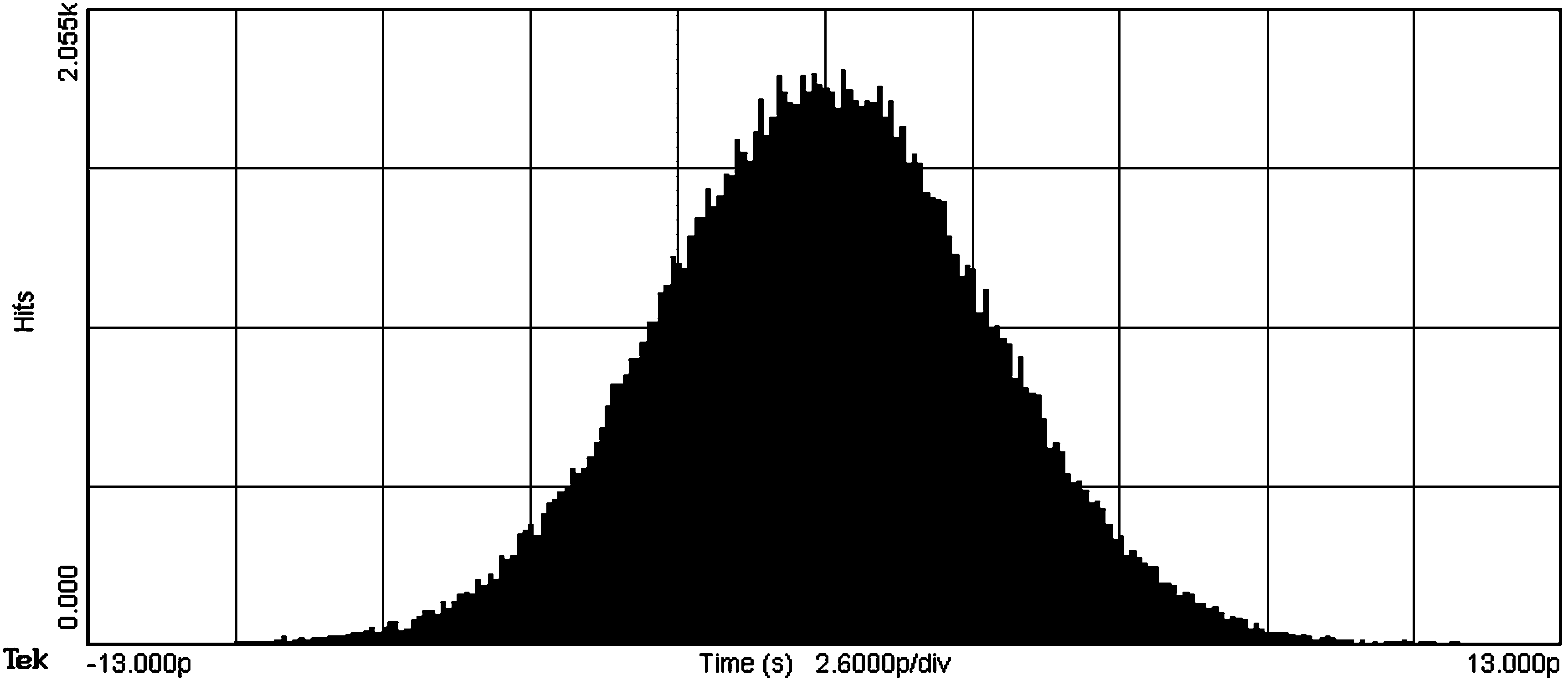
| Horizontal Scale: 2.6ps / Division | ||
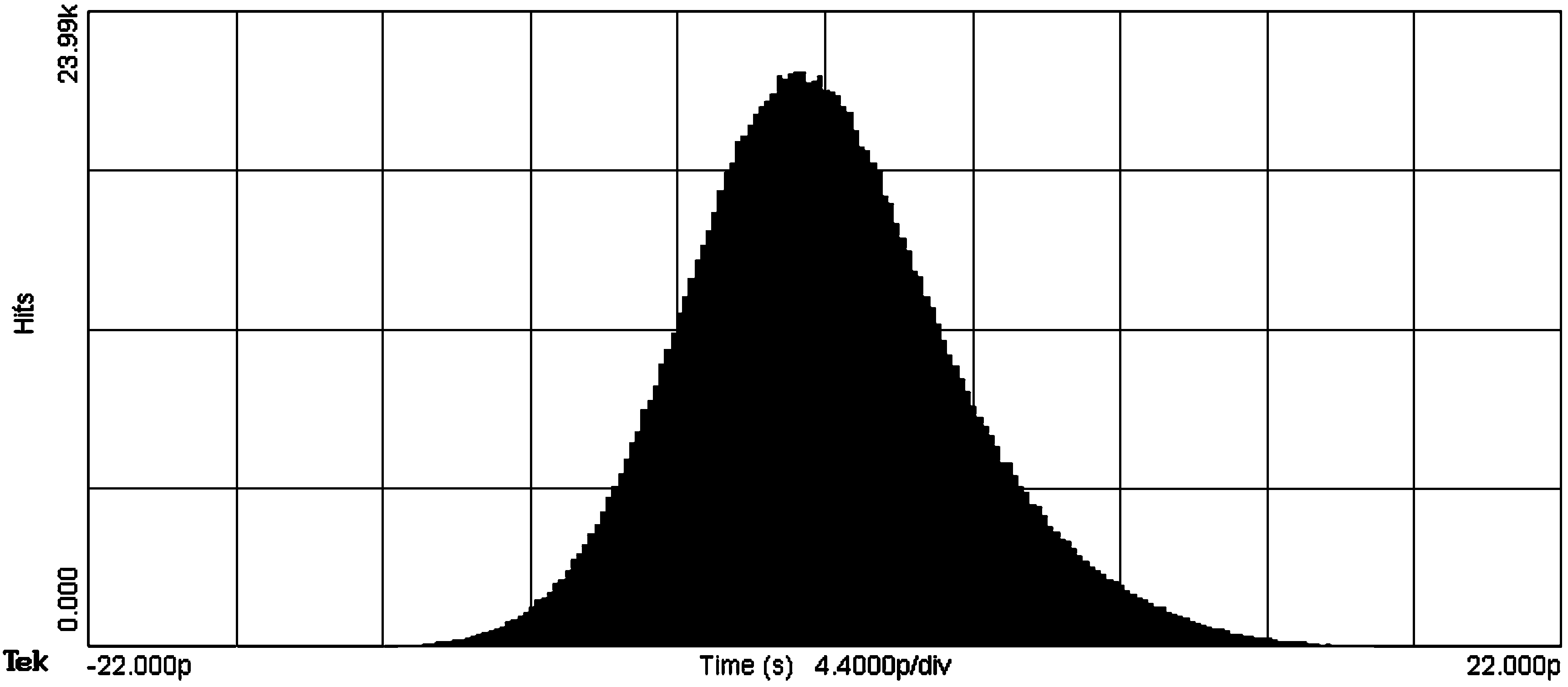
| Horizontal Scale: 4.4ps / Division | ||
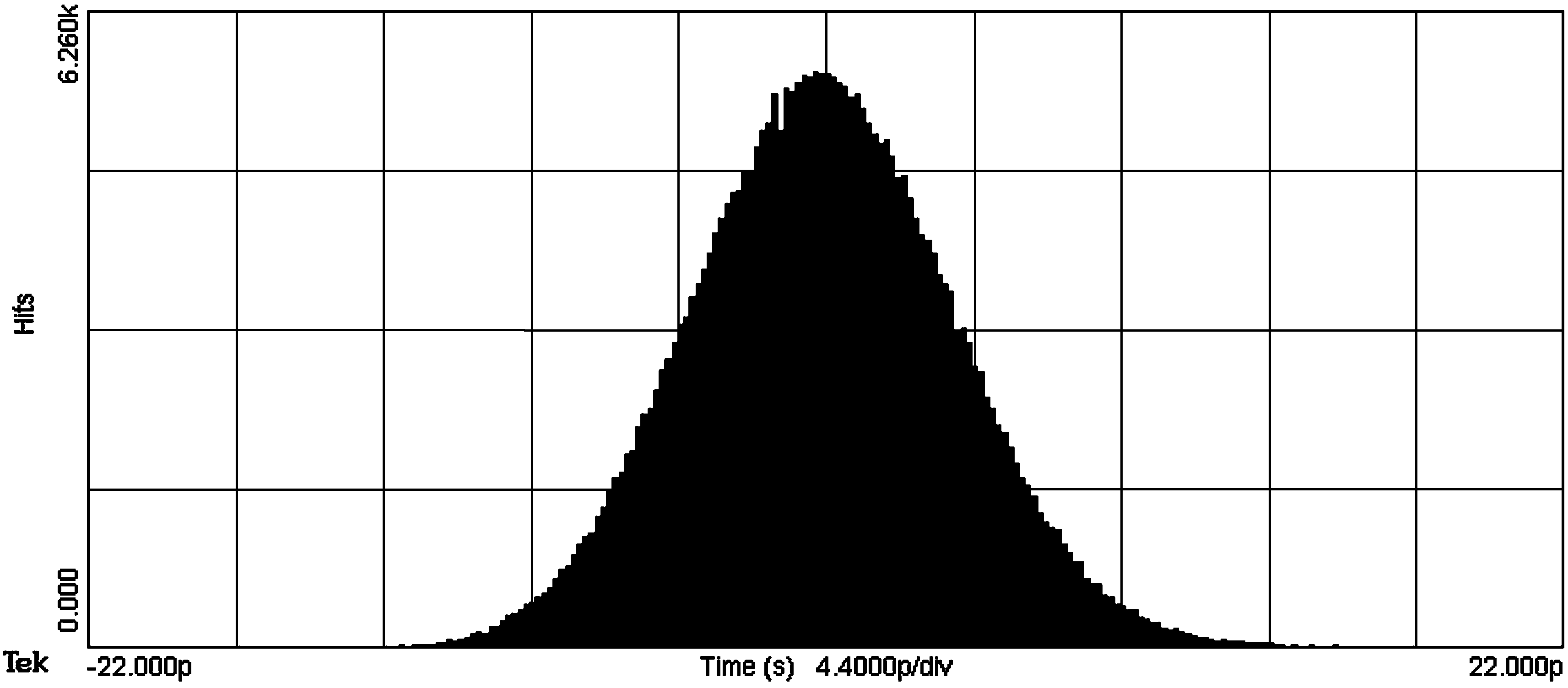
| Horizontal Scale: 4.4ps / Div | ||
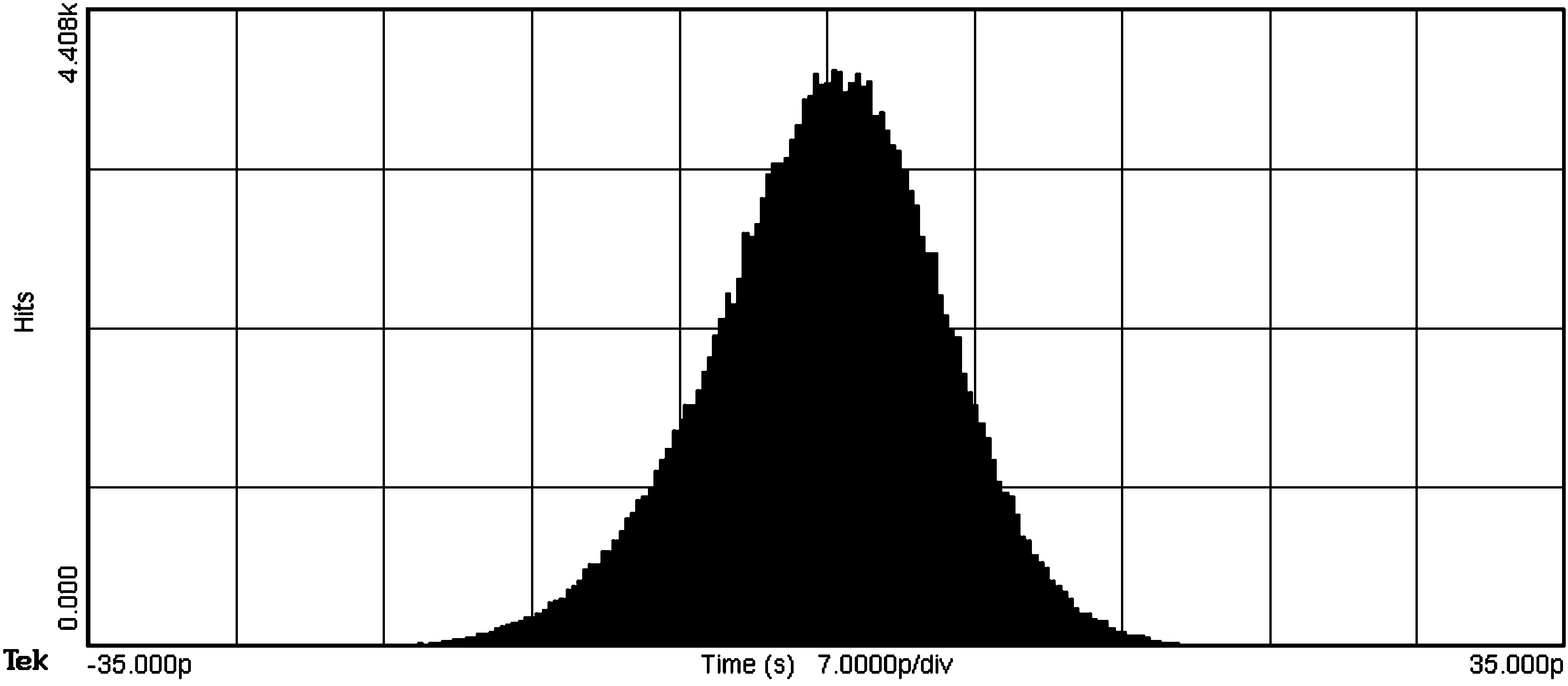
| Horizontal Scale: 7 ps / Div | ||