SBOS965D October 2019 – January 2023 LMH32401
PRODUCTION DATA
- 1 Features
- 2 Applications
- 3 Description
- 4 Revision History
- 5 Pin Configuration and Functions
-
6 Specifications
- 6.1 Absolute Maximum Ratings
- 6.2 ESD Ratings
- 6.3 Recommended Operating Conditions
- 6.4 Thermal Information
- 6.5 Electrical Characteristics: Gain = 2 kΩ
- 6.6 Electrical Characteristics: Gain = 20 kΩ
- 6.7 Electrical Characteristics: Both Gains
- 6.8 Electrical Characteristics: Logic Threshold and Switching Characteristics
- 6.9 Typical Characteristics
- 7 Detailed Description
- 8 Application and Implementation
- 9 Power Supply Recommendations
- 10Layout
- 11Device and Documentation Support
- 12Mechanical, Packaging, and Orderable Information
Package Options
Refer to the PDF data sheet for device specific package drawings
Mechanical Data (Package|Pins)
- RGT|16
- Y|0
Thermal pad, mechanical data (Package|Pins)
- RGT|16
Orderable Information
7.3.4 Differential Output Stage
The differential output stage of the LMH32401 device performs the following two functions, which are common across all differential amplifiers:
- Converts the single-ended output from the TIA stage to a differential output.
- Performs a common-mode output shift to match the specified ADC input common-mode voltage.
The differential output stage has two 10-Ω series resistors on its output to isolate the amplifier output stage transistors from the package bond-wire inductance and printed circuit board (PCB) capacitance. The net gain of the LMH32401 device (TIA + output stage) is 2 kΩ (low gain) and 20 kΩ (high gain) when driving an external 100-Ω resistor. When the external load resistor is increased above 100 Ω, the effective gain from the IN pin to the differential output pin increases. Conversely, when the external load resistor is decreased to less than 100 Ω, the effective gain from the IN pin to the differential output pin decreases as a result of the larger voltage drop across the two internal 10-Ω resistors. When there is no load resistor between the OUT+ and OUT– pins, the effective gain of the LMH32401 is 2.4 kΩ and 24 kΩ in the low-gain and high-gain configurations, respectively.
The output common-mode voltage of the LMH32401 device can be set externally through the VOCM pin. A resistor divider internal to the amplifier, between VDD2 and ground sets the default voltage to 1.1 V. The internal resistors generate common-mode noise that is typically rejected by the CMRR of the subsequent ADC stage. To maximize the amplifier signal-to-noise ratio (SNR), place an external noise bypass capacitor to ground on the VOCM pin. In single-ended signal chains, such as ToF systems that use time-to-digital converters (TDCs), only a single output of the LMH32401 device is needed. In such situations, terminate the unused differential output in the same manner as the used output to maintain balance and symmetry. The signal swing of the single-ended output is half the available differential output swing. Additionally, the common-mode noise of the output stage, which is typically rejected by the differential input ADC, is now added to the total noise, further degrading SNR.
The output stage of the LMH32401 device has an additional VOD input that sets the differential output between OUT– and OUT+. Figure 7-1 shows how each output pin of the LMH32401 device is at the voltage set by the VOCM pin (default = 1.1 V) when the photodiode output current is zero and the VOD input is set to 0 V. When the VOD pin is driven to a voltage of X volts, the two output pins are separated by X volts when the photodiode current is zero. The average voltage is still equal to VOCM. For example, Figure 7-2 shows if VOCM is set to 1.1 V and VOD is set to 0.4 V, then OUT– = 1.1 V + 0.2 V = 1.3 V and OUT+ = 1.1 V – 0.2 V = 0.9 V.
The VOD pin is functional only when the LMH32401 device is used with a PD that sinks the photocurrent. Set VOD = 0 V when the LMH32401 device is interfaced with a PD that sources the photocurrent. The VOD output offset feature is included in the LMH32401 device because the output current of a photodiode is unipolar. Depending on the reverse bias configuration, the photodiode can either sink or source current, but cannot do both at the same time. With the anode connected to a negative bias and the cathode connected to the TIA stage input, the photodiode can only sink current, which implies that the TIA stage output swings in a positive direction above its default input bias voltage (2.47 V). Subsequently, OUT– only swings below VOCM and OUT+ only swings above VOCM. Figure 7-1 shows how the LMH32401 device only uses half of its output swing range (VOUT = VOUT+ – VOUT–) when VOD = 0 V, because one output never swings below VOCM and the other output never goes above VOCM. The signal dynamic range in this case is 0.4 VPP – 0 V = 0.4 VPP.
Figure 7-2 shows how the VOD pin voltage allows OUT– to be level-shifted above VOCM and OUT+ to be level-shifted below VOCM to maximize the output swing capabilities of the amplifier. The signal dynamic range in this case is 0.4 VPP – (–0.4 VPP) = 0.8 VPP.
 Figure 7-1 Individual Single-Ended Outputs With VOD = 0 V
 Figure 7-2 Individual Single-Ended Outputs With VOD = 0.4 V
When the LMH32401 device drives a 100-Ω load, the voltage set at the VOD pin is equal to the differential output offset (VOUT = VOUT+ – VOUT–) when the input signal current is zero. Use Equation 1 to calculate the differential output offset under other load conditions.
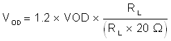
Where:
- VOD = Voltage applied at pin 9
- VOD = (VOUT– – VOUT+)
- RL = External load resistance