SNOS966Q May 2001 – September 2014 LMH6642 , LMH6643 , LMH6644
PRODUCTION DATA.
- 1 Features
- 2 Applications
- 3 Description
- 4 Revision History
- 5 Description (continued)
- 6 Pin Configuration and Functions
- 7 Specifications
- 8 Detailed Description
- 9 Application and Implementation
- 10Power Supply Recommendations
- 11Layout
- 12Device and Documentation Support
- 13Mechanical, Packaging, and Orderable Information
Package Options
Mechanical Data (Package|Pins)
Thermal pad, mechanical data (Package|Pins)
Orderable Information
9 Application and Implementation
NOTE
Information in the following applications sections is not part of the TI component specification, and TI does not warrant its accuracy or completeness. TI’s customers are responsible for determining suitability of components for their purposes. Customers should validate and test their design implementation to confirm system functionality.
9.1 Application Information
This device family was designed to avoid output phase reversal. With input overdrive, the output is kept near supply rail (or as closed to it as mandated by the closed loop gain setting and the input voltage). See Figure 56.
However, if the input voltage range of −0.5 V to 1 V from V+ is exceeded by more than a diode drop, the internal ESD protection diodes will start to conduct. The current in the diodes should be kept at or below 10 mA.
Output overdrive recovery time is less than 100 ns as can be seen in Figure 57.
9.2 Typical Application
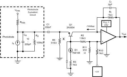 Figure 55. Single Supply Photodiode I-V Converter
9.2.1 Design Requirements
The circuit shown in Figure 55 is used to amplify the current from a photodiode into a voltage output. In this circuit, the emphasis is on achieving high bandwidth and the transimpedance gain setting is kept relatively low. Because of its high slew rate limit and high speed, the LMH664X family lends itself well to such an application. This circuit achieves approximately 1V/mA of transimpedance gain and capable of handling up to 1mApp from the photodiode. Q1, in a common base configuration, isolates the high capacitance of the photodiode (Cd) from the Op Amp input in order to maximize speed. Input is AC coupled through C1 to ease biasing and allow single supply operation. With 5-V single supply, the device input/output is shifted to near half supply using a voltage divider from VCC. Note that Q1 collector does not have any voltage swing and the Miller effect is minimized. D1, tied to Q1 base, is for temperature compensation of Q1’s bias point. Q1 collector current was set to be large enough to handle the peak-to-peak photodiode excitation and not too large to shift the U1 output too far from mid-supply.
9.2.1.1 Input and Output Topology
All input / output pins are protected against excessive voltages by ESD diodes connected to V+ and V- rails (see Figure 54). These diodes start conducting when the input / output pin voltage approaches 1Vbe beyond V+ or V- to protect against over voltage. These diodes are normally reverse biased. Further protection of the inputs is provided by the two resistors (R in Figure 54), in conjunction with the string of anti-parallel diodes connected between both bases of the input stage. The combination of these resistors and diodes reduces excessive differential input voltages approaching 2Vbe. This occurs most commonly when the device is used as a comparator (or with little or no feedback) and the device inputs no longer follow each other. In such a case, the diodes may conduct. As a consequence, input current increases and the differential input voltage is clamped. It is important to make sure that the subsequent current flow through the device input pins does not violate the Absolute Maximum Ratings of the device. To limit the current through this protection circuit, extra series resistors can be placed. Together with the built-in series resistors of several hundred ohms, these external resistors can limit the input current to a safe number (that is, less than 10mA). Be aware that these input series resistors may impact the switching speed of the device and could slow down the device.
9.2.1.2 Single Supply, Low Power Photodiode Amplifier
The circuit shown in Figure 55 is used to amplify the current from a photodiode into a voltage output. In this circuit, the emphasis is on achieving high bandwidth and the transimpedance gain setting is kept relatively low. Because of its high slew rate limit and high speed, the LMH664X family lends itself well to such an application.
This circuit achieves approximately 1V/mA of transimpedance gain and capable of handling up to 1mApp from the photodiode. Q1, in a common base configuration, isolates the high capacitance of the photodiode (Cd) from the Op Amp input in order to maximize speed. Input is AC coupled through C1 to ease biasing and allow single supply operation. With 5V single supply, the device input/output is shifted to near half supply using a voltage divider from VCC. Note that Q1 collector does not have any voltage swing and the Miller effect is minimized. D1, tied to Q1 base, is for temperature compensation of Q1’s bias point. Q1 collector current was set to be large enough to handle the peak-to-peak photodiode excitation and not too large to shift the U1 output too far from mid-supply.
No matter how low an Rf is selected, there is a need for Cf in order to stabilize the circuit. The reason for this is that the Op Amp input capacitance and Q1 equivalent collector capacitance together (CIN) will cause additional phase shift to the signal fed back to the inverting node. Cf will function as a zero in the feedback path counter-acting the effect of the CIN and acting to stabilized the circuit. By proper selection of Cf such that the Op Amp open loop gain is equal to the inverse of the feedback factor at that frequency, the response is optimized with a theoretical 45° phase margin.
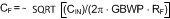
where
- GBWP is the Gain Bandwidth Product of the Op Amp
Optimized as such, the I-V converter will have a theoretical pole, fp, at:
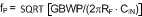
With Op Amp input capacitance of 3pF and an estimate for Q1 output capacitance of about 3pF as well, CIN = 6 pF. From the typical performance plots, LMH6642/6643 family GBWP is approximately 57 MHz. Therefore, with Rf = 1k, from Equation 1 and Equation 2:
For this example, optimum Cf was empirically determined to be around 5 pF. This time domain response is shown in Figure 58 below showing about 9 ns rise/fall times, corresponding to about 39 MHz for fp. The overall supply current from the +5 V supply is around 5 mA with no load.
9.2.2 Detailed Design Procedure
No matter how low an Rf is selected, there is a need for Cf in order to stabilize the circuit. The reason for this is that the Op Amp input capacitance and Q1 equivalent collector capacitance together (CIN) will cause additional phase shift to the signal fed back to the inverting node. Cf will function as a zero in the feedback path counteracting the effect of the CIN and acting to stabilized the circuit. By proper selection of Cf such that the Op Amp open loop gain is equal to the inverse of the feedback factor at that frequency, the response is optimized with a theoretical 45° phase margin where GBWP is the Gain Bandwidth Product of the Op Amp, Optimized as such, the I-V converter will have a theoretical pole, fp, at: (2) With Op Amp input capacitance of 3pF and an estimate for Q1 output capacitance of about 3pF as well, CIN = 6 pF. From the typical performance plots, LMH6642/6643 family GBWP is approximately 57 MHz. Therefore, with Rf = 1k, from Equation 2 and Equation 3 : Cf = ∼4.1 pF and fp = 39 MHz.
Single Supply Photodiode I-V Converter For this example, optimum Cf was empirically determined to be around 5 pF. This time domain response is shown in Figure 58 showing about 9 ns rise/fall times, corresponding to about 39 MHz for fp. The overall supply current from the +5 V supply is around 5 mA with no load.
9.2.3 Application Curves
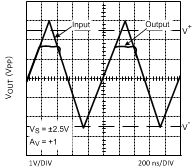 Figure 56. Input and Output Shown with CMVR Exceeded
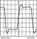 Figure 58. Converter Step Response (1VPP, 20 ns/DIV)
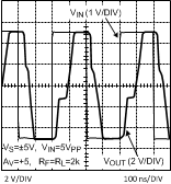 Figure 57. Overload Recovery Waveform