SNOS966Q May 2001 – September 2014 LMH6642 , LMH6643 , LMH6644
PRODUCTION DATA.
- 1 Features
- 2 Applications
- 3 Description
- 4 Revision History
- 5 Description (continued)
- 6 Pin Configuration and Functions
- 7 Specifications
- 8 Detailed Description
- 9 Application and Implementation
- 10Power Supply Recommendations
- 11Layout
- 12Device and Documentation Support
- 13Mechanical, Packaging, and Orderable Information
Package Options
Mechanical Data (Package|Pins)
Thermal pad, mechanical data (Package|Pins)
Orderable Information
8 Detailed Description
8.1 Overview
The LMH664X family is based on proprietary VIP10 dielectrically isolated bipolar process. This device family architecture features the following:
- Complimentary bipolar devices with exceptionally high ft (∼8 GHz) even under low supply voltage (2.7 V) and low bias current.
- A class A-B “turn-around” stage with improved noise, offset, and reduced power dissipation compared to similar speed devices (patent pending).
- Common Emitter push-push output stage capable of 75 mA output current (at 0.5 V from the supply rails) while consuming only 2.7 mA of total supply current per channel. This architecture allows output to reach within mV of either supply rail.
- Consistent performance over the entire operating supply voltage range with little variation for the most important specifications (for example, BW, SR, IOUT, and so forth)
- Significant power saving (∼40%) compared to competitive devices on the market with similar performance.
8.2 Functional Block Diagram
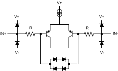 Figure 54. Input Equivalent Circuit
8.3 Feature Description
The LMH664X family is a drop-in replacement for the AD805X family of high speed Op Amps in most applications. In addition, the LMH664X will typically save about 40% on power dissipation, due to lower supply current, when compared to competition. All AD805X family’s specified parameters are included in the list of LMH664X ensured specifications in order to ensure equal or better level of performance. However, as in most high performance parts, due to subtleties of applications, it is strongly recommended that the performance of the part to be evaluated is tested under actual operating conditions to ensure full compliance to all specifications.
8.4 Device Functional Modes
With 3-V supplies and a common mode input voltage range that extends 0.5 V below V−, the LMH664X find applications in low voltage/low power applications. Even with 3-V supplies, the −3dB BW (@ AV = +1) is typically 115 MHz with a tested limit of 80 MHz. Production testing guarantees that process variations will not compromise speed. High frequency response is exceptionally stable, confining the typical −3dB BW over the industrial temperature range to ±2.5%.
As seen in Typical Performance Characteristics, the LMH664X output current capability (∼75 mA) is enhanced compared to AD805X. This enhancement increases the output load range, adding to the LMH664X’s versatility. Since LMH664X is capable of high output current, device junction temperature should not to exceed the Absolute Maximum Ratings.