SNOS966Q May 2001 – September 2014 LMH6642 , LMH6643 , LMH6644
PRODUCTION DATA.
- 1 Features
- 2 Applications
- 3 Description
- 4 Revision History
- 5 Description (continued)
- 6 Pin Configuration and Functions
- 7 Specifications
- 8 Detailed Description
- 9 Application and Implementation
- 10Power Supply Recommendations
- 11Layout
- 12Device and Documentation Support
- 13Mechanical, Packaging, and Orderable Information
Package Options
Mechanical Data (Package|Pins)
Thermal pad, mechanical data (Package|Pins)
Orderable Information
11 Layout
11.1 Layout Guidelines
Generally, a good high frequency layout will keep power supply and ground traces away from the inverting input and output pins. Parasitic capacitances on these nodes to ground will cause frequency response peaking and possible circuit oscillations (see Application Note OA-15, "Frequent Faux Pas in Applying Wideband Current Feedback Amplifiers", SNOA367, for more information). Texas Instruments suggests the following evaluation boards as a guide for high frequency layout and as an aid in device testing and characterization:
Table 1. Printed Circuit Board Layout And Component Values
| DEVICE | PACKAGE | EVALUATION BOARD PN |
|---|---|---|
| LMH6642MF | 5-Pin SOT-23 | LMH730216 |
| LMH6642MA | 8-Pin SOIC | LMH730227 |
| LMH6643MA | 8-Pin SOIC | LMH730036 |
| LMH6643MM | 8-Pin VSSOP | LMH730123 |
| LMH6644MA | 14-Pin SOIC | LMH730231 |
| LMH6644MT | 14-Pin TSSOP | LMH730131 |
Another important parameter in working with high speed/high performance amplifiers, is the component values selection. Choosing external resistors that are large in value will effect the closed loop behavior of the stage because of the interaction of these resistors with parasitic capacitances. These capacitors could be inherent to the device or a by-product of the board layout and component placement. Either way, keeping the resistor values lower, will diminish this interaction to a large extent. On the other hand, choosing very low value resistors could load down nodes and will contribute to higher overall power dissipation.
11.2 Layout Example
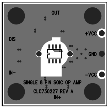 Figure 59. LMH6642/LMH6643/LMH6644 Layer 1
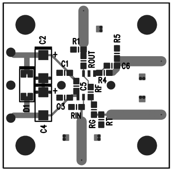 Figure 60. LMH6642/LMH6643/LMH6644 Layer 2