SNOSA35G August 2002 – July 2015 LMH6657 , LMH6658
PRODUCTION DATA.
- 1 Features
- 2 Applications
- 3 Description
- 4 Revision History
- 5 Pin Configuration and Functions
- 6 Specifications
- 7 Detailed Description
- 8 Application and Implementation
- 9 Power Supply Recommendations
- 10Layout
- 11Device and Documentation Support
- 12Mechanical, Packaging, and Orderable Information
Package Options
Mechanical Data (Package|Pins)
Thermal pad, mechanical data (Package|Pins)
Orderable Information
7 Detailed Description
7.1 Overview
7.1.1 Large Signal Behavior
The LMH6657 and LMH6658 are large-bandwidth, fast slew rate, voltage feedback operational ampplifers ideal for high-speed, large signal applications. The low input referred voltage noise in conjunction with an input voltage range, which extends below V–, eases the adoption of this part in applications having a tiny signal at or near system ground, as well as other high-speed, low-distortion, and low-noise systems. Also, the large Gain Bandwidth Product allows high gain operation that does not compromise speed.
7.2 Feature Description
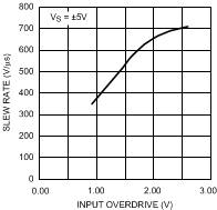
The LMH6657 and LMH6658 input stage is designed to provide excess overdrive when needed. This occurs when fast input signal excursions cannot be followed by the output stage. In these situations, the device encounters larger input signals than would be encountered under normal closed loop conditions. The LMH6657 and LMH6658 input stage is designed to take advantage of this "input overdrive" condition. The larger the amount of this overdrive, the greater is the speed with which the output voltage can change. Here is a plot of how the output slew rate limitation varies with respect to the amount of overdrive imposed on the input:
 Figure 48. Plot Showing the Relationship Between Slew Rate and Input Overdrive
To relate the explanation above to a practical example, consider the following application example. Consider the case of a closed loop amplifier with a gain of −1 amplifying a sinusoidal waveform. From the plot of Output vs. Input (Figure 8), with a 30-MHz signal and 7VPP input signal, it can be seen that the output will be limited to a swing of 6.9 VPP. From the frequency Response plot it can be seen that the inverting gain of −1 has a −32° output phase shift at this frequency.
It can be shown that this setup will result in about 1.9 VPP differential input voltage corresponding to 650 V/μs of slew rate from Figure 48, above (SR = VO(pp) × π × f = 650V/μs)
Note that the amount of overdrive appearing on the input for a given sinusoidal test waveform is affected by the following:
- Output swing
- Gain setting
- Input/output phase relationship for the given test frequency
- Amplifier configuration (inverting or noninverting)
Due to the higher frequency phase shift between input and output, there is no closed form solution to input overdrive for a given input. Therefore, Figure 48 is not very useful by itself in determining the output swing.
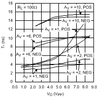
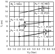
The following plots aid in predicting the output transition time based on the amount of swing required for a given gain setting.
 Figure 49. Output 20%-80% Transition vs. Output Voltage Swing (Noninverting Gain)
 Figure 50. Output 20%-80% Transition vs. Output Voltage Swing (Inverting Gain)
Beyond a gain of 5 or so, the LMH6657/6658 output transition would be limited by bandwidth. For example, with a gain of 5, the −3dB BW would be around 30MHz corresponding to a rise time of about 12ns (10% - 90%). Assuming a near linear transition, the 20%-80% transition time would be around 9ns which matches the measured results as shown in Figure 49.
When the output is heavily loaded, output swing may be limited by current capability of the device. Refer to Output Current Capability section for more details.
7.3 Device Functional Modes
7.3.1 Output Phase Reversal
This is a problem with some operational amplifiers. This effect is caused by phase reversal in the input stage due to saturation of one or more of the transistors when the inputs exceed the normal expected range of voltages. Some applications, such as servo control loops among others, are sensitive to this kind of behavior and would need special safeguards to ensure proper functioning. The LMH6657 and LMH6658 is immune to output phase reversal with input overload. With inputs exceeded, the LMH6657 and LMH6658 output will stay at the clamped voltage from the supply rail. Exceeding the input supply voltages beyond the Absolute Maximum Ratings of the device could however damage or otherwise adversely effect the reliability or life of the device.