SNOSC84D August 2012 – February 2015 LMH6882
PRODUCTION DATA.
- 1 Features
- 2 Applications
- 3 Description
- 4 Revision History
- 5 Pin Configuration and Functions
- 6 Specifications
- 7 Detailed Description
- 8 Application and Implementation
- 9 Power Supply Recommendations
- 10Layout
- 11Device and Documentation Support
- 12Mechanical, Packaging, and Orderable Information
Package Options
Refer to the PDF data sheet for device specific package drawings
Mechanical Data (Package|Pins)
- NJK|36
Thermal pad, mechanical data (Package|Pins)
Orderable Information
8 Application and Implementation
NOTE
Information in the following applications sections is not part of the TI component specification, and TI does not warrant its accuracy or completeness. TI’s customers are responsible for determining suitability of components for their purposes. Customers should validate and test their design implementation to confirm system functionality.
8.1 Application Information
8.1.1 Input Characteristics
The LMH6882 has internally terminated inputs. The INMD and INPD pins are intended to be the differential input pins and have an internal 100-Ω resistive termination. An example differential circuit is shown in Figure 39. When using the differential inputs, the single-ended inputs should be left disconnected.
The INMS and INPS pins are intended for use as single-ended inputs and have been designed to support single-ended termination of 50 Ω working as an active termination. For single-ended signals an external 50-Ω resistor is required as shown in Figure 40. When using the single-ended inputs, the differential inputs should be left disconnected.
All of the input pins are self biased to 2.5 V. When using the LMH6882 for DC-coupled applications, it is possible to externally bias the input pins to voltages from 1.5 V to 3.5 V. Performance is best at the 2.5-V level specified. Performance will degrade slightly as the common mode shifts away from 2.5 V.
The first stage of the LMH6882 is a low-noise amplifier that can accommodate a maximum input signal of 2 Vppd on the differential input pins and 1 Vpp on either of the single-ended pins. Signals larger than this will cause severe distortion. Although the inputs are protected against ESD, sustained electrical overstress will damage the part. Signal power over 13 dBm should not be applied to the amplifier differential inputs continuously. On the single-ended pins the power limit is 10 dBm for each pin.
8.1.2 Output Characteristics
The LMH6882 has a low-impedance output very similar to a traditional Op-amp output. This means that a wide range of loads can be driven with good performance. Matching load impedance for proper termination of filters is as easy as inserting the proper value of resistor between the filter and the amplifier (See Figure 50 for example.) This flexibility makes system design and gain calculations very easy. By using a differential output stage the LMH6882 can achieve large voltage swings on a single 5-V supply. This is illustrated in Figure 45. This figure shows how a voltage swing of 4 Vppd is realized while only swinging 2 Vpp on each output. A 1-Vp signal on one branch corresponds to 2 Vpp on that branch and 4 Vppd when looking at both branches (positive and negative).
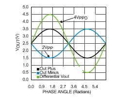 Figure 45. Differential Output Voltage
The LMH6882 has been designed for both AC-coupled and DC-coupled applications. To give more flexibility in DC-coupled applications, the common-mode voltage of the output pins is set by the OCM pin. The OCM pin needs to be driven from an external low-noise source. If the OCM pin is left floating, the output common-mode is undefined, and the amplifier will not operate properly.
There is a DC gain of 2 between the OCM pin and the output pins so that the OCM voltage should be between 1 V and 1.5 V. This will set the output common mode voltage between 2 V and 3 V. Output common-mode voltages outside the recommended range will exhibit poor voltage swing and distortion performance. The amplifier will give optimum performance when the output common mode is set to half of the supply voltage (2.5 V or 1.25 V at the OCM pin).
The ability of the LMH6882 to drive low-impedance loads while maintaining excellent OIP3 performance creates an opportunity to greatly increase power gain and drive low-impedance filters. This gives the system designer much needed flexibility in filter design. In many cases using a lower impedance filter will provide better component values for the filter. Another benefit of low-impedance filters is that they are less likely to be influenced by circuit board parasitic reactances such as pad capacitance or trace inductance. The output stage is a low-impedance voltage amplifier, so voltage gain is constant over different load conditions. Power gain will change based on load conditions. See Figure 46 for details on power gain with respect to different load conditions. The graph was prepared for the 26 dB voltage gain. Other gain settings will behave similarly.
All measurements in this data sheet, unless specified otherwise, refer to voltage or power at the device output pins. For instance, in an OIP3 measurement the power out will be equal to the output voltage at the device pins squared, divided by the total load voltage. In back-terminated applications, power to the load would be 3 dB less. Common back-terminated applications include driving a matched filter or driving a transmission line.
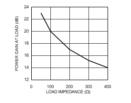 Figure 46. Power Gain as a Function of the Load
Printed circuit board (PCB) design is critical to high-frequency performance. In order to ensure output stability the load-matching resistors should be placed as close to the amplifier output pins as possible. This allows the matching resistors to mask the board parasitics from the amplifier output circuit. An example of this is shown in Figure 50. Also note that the low-pass filters in Figure 48 and Figure 49 use center-tapped capacitors. Having capacitors to ground provides a path for high-frequency, common-mode energy to dissipate. This is equally valuable for the ADC, so there are also capacitors to ground on the ADC side of the filter. The LMH6882EVAL evaluation board is available to serve a guide for system board layout. See also application note AN-2235 (SNOA869) for more details.
8.1.3 Interfacing to an ADC
The LMH6882 is an excellent choice for driving high-speed ADCs such as the ADC12D1800RF, ADC12D1600RF or the ADS5400. The following sections will detail several elements of ADC system design, including noise filters, AC, and DC coupling options.
8.1.3.1 ADC Noise Filter
When connecting a broadband amplifier to an analog to digital converter it is nearly always necessary to filter the signal before sampling it with the ADC. Figure 47 shows a schematic of a second order Butterworth filter and Table 8 shows component values for some common IF frequencies. These filters, shown in Table 8, offer a good compromise between bandwidth, noise rejection and cost. This filter topology is the same as is used on the ADC14V155KDRB High IF Receiver reference design board. This filter topology is adequate for reducing aliasing of broadband noise and will also provide rejection of harmonic distortion and many of the images that are commonly created by mixers.
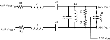 Figure 47. Sample Filter
Table 8. Filter Component Values(1)
| CENTER FREQUENCY | BANDWIDTH | R1, R2 | L1, L2 | C1, C2 | C3 | L5 | R3, R4 |
|---|---|---|---|---|---|---|---|
| 75 MHz | 40 MHz | 90 Ω | 390 nH | 10 pF | 22 pF | 220 nH | 100 Ω |
| 150 MHz | 60 MHz | 90 Ω | 370 nH | 3 pF | 19 pF | 62 nH | 100 Ω |
| 180 MHz | 75 MHz | 90 Ω | 300 nH | 2.7 pF | 15 pF | 54 nH | 100 Ω |
| 250 MHz | 100 MHz | 90 Ω | 225 nH | 1.9 pF | 11 pF | 36 nH | 100 Ω |
8.1.3.2 AC Coupling to an ADC
AC coupling is an effective method for interfacing to an ADC for many communications systems. In many applications this will be the best choice. The LMH6882 evaluation board is configured for AC coupling as shipped from the factory. Coupling with capacitors is usually the most cost-effective method. Transformers can provide both AC coupling and impedance transformation as well as single-ended-to-differential conversion. One of the key benefits of AC coupling is that each stage of the system can be biased to the ideal DC operating point. Many systems operate with lower overall power dissipation when DC bias currents are eliminated between stages.
8.1.3.3 DC Coupling to an ADC
The LMH6882 supports DC-coupled signals. In order to successfully implement a DC-coupled signal chain the common-mode voltage requirements of every stage need to be met. This requires careful planning, and in some cases there will be signal-level, gain or termination compromises required to meet the requirements of every part. Shown in Figure 48 and Figure 49 is a method using resistors to change the 2.5-V common mode of the amplifier output to a common mode compatible for the input of a low-input voltage ADC such as the ADC12D1800RF. This DC level shift is achieved while maintaining an AC impedance match with the filter in Figure 48 while in Figure 49 there is a small mismatch between the amplifier termination resistors and the ADC input. Because there is no universal ADC input common mode, and some ADC’s have impedance controlled input, each design will require a different resistor ratio. For high-speed data-conversion systems it is very important to keep the physical distance between the amplifier and the ADC electrically short. When connections between the amplifier and the ADC are electrically short, termination mismatches are not critical.
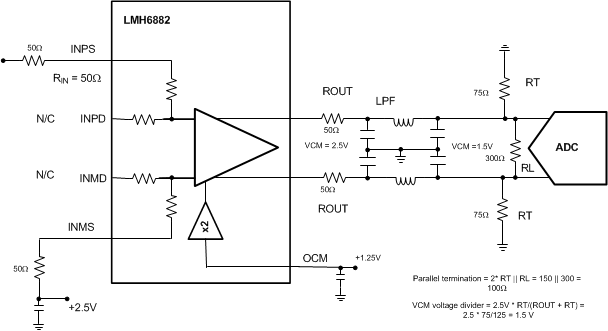 Figure 48. DC-Coupled ADC Driver Example 1, High Input Impedance ADC
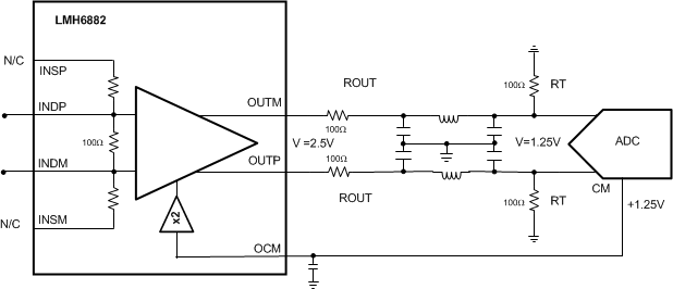 Figure 49. DC-Coupled ADC Driver Example 2, ADC12D1800RF with Terminated Input
8.1.4 Figure of Merit: Dynamic Range Figure
The dynamic range figure (DRF) as illustrated in Figure 4, is defined as the input third order intercept point (IIP3) minus the noise figure (NF). The combination of noise figure and linearity gives a good proxy for the total dynamic range of an amplifier. In some ways this figure is similar to the SFDR of an analog to digital converter. In contrast to an ADC, however, an amplifier will not have a full-scale input to use as a reference point. With amplifiers, there is no one point where signal amplitude hits “full scale”. Yet, there are real limitations to how large a signal the amplifier can handle. Normally, the distortion products produced by the amplifier will determine the upper limit to signal amplitude. The intermodulation intercept point is an imaginary point that gives a well-understood figure of merit for the maximum signal an amplifier can handle. For low-amplitude signals the noise figure gives a threshold of the lowest signal that the amplifier can reproduce. By combining the third-order input intercepts point and the noise figure the DRF gives a very good indication of the available dynamic range offered.
Table 9. Compatible High-Speed Analog-to-Digital Converters
| PRODUCT NUMBER | MAX SAMPLING RATE (MSPS) | RESOLUTION | CHANNELS |
|---|---|---|---|
| ADC12D1800RF | 1800 | 12 | DUAL |
| ADC12D1600RF | 1600 | 12 | DUAL |
| ADC12D1000RF | 1000 | 12 | DUAL |
| ADS5400 | 1000 | 12 | SINGLE |
| ADC12D1800 | 1800 | 12 | DUAL |
| ADC12D1600 | 1600 | 12 | DUAL |
| ADC12D1000 | 1000 | 12 | DUAL |
| ADC10D1000 | 1000 | 10 | DUAL |
| ADC10D1500 | 1500 | 10 | DUAL |
| ADC12C105 | 105 | 12 | SINGLE |
| ADC12C170 | 170 | 12 | SINGLE |
| ADC12V170 | 170 | 12 | SINGLE |
| ADC14C080 | 80 | 14 | SINGLE |
| ADC14C105 | 105 | 14 | SINGLE |
| ADC14DS105 | 105 | 14 | DUAL |
| ADC14155 | 155 | 14 | SINGLE |
| ADC14V155 | 155 | 14 | SINGLE |
| ADC16V130 | 130 | 16 | SINGLE |
| ADC16DV160 | 160 | 16 | DUAL |
| ADC08D500 | 500 | 8 | DUAL |
| ADC08500 | 500 | 8 | SINGLE |
| ADC08D1000 | 1000 | 8 | DUAL |
| ADC081000 | 1000 | 8 | SINGLE |
| ADC08D1500 | 1500 | 8 | DUAL |
| ADC081500 | 1500 | 8 | SINGLE |
| ADC08(B)3000 | 3000 | 8 | SINGLE |
| ADC08100 | 100 | 8 | SINGLE |
| ADCS9888 | 170 | 8 | SINGLE |
| ADC08(B)200 | 200 | 8 | SINGLE |
| ADC11C125 | 125 | 11 | SINGLE |
| ADC11C170 | 170 | 11 | SINGLE |
8.2 Typical Applications
8.2.1 LMH6882 Typical Application
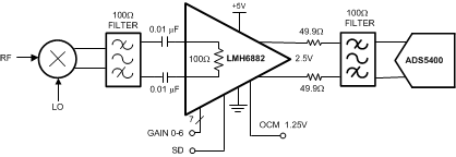 Figure 50. LMH6882 Typical Application
8.2.1.1 Design Requirements
Figure 50 shows a design example for an IF amplifier in a typical direct-IF receiver application and LMH6881 meets these requirements.
Table 10. Example Design Requirement for an IF Receiver Application
| SPECIFICATION | EXAMPLE DESIGN REQUIREMENT |
|---|---|
| Supply Voltage and Current | 4.75V to 5.25V, with a minimum 150-mA supply current |
| Input structure and Impedance | DC coupled Single-ended or Differential with 100Ω input differential impedance |
| Output control | DC coupled with output common mode control capability |
| RF input frequency range | DC to 250MHz |
| Voltage Gain Range | 26dB to 6dB |
| OIP3 in RF input frequency range for Pout = 4dBm/tone with RL = 200Ω | > 38 dBm at 200MHz for Max Gain |
| Noise Figure | < 12dB at Max Gain across RF input frequency |
| Attenuation Control | Parallel control as well as SPI control |
8.2.1.2 Detailed Design Procedure
The LMH6882 device can be included in most receiver applications by following these basic procedures:
- Select an appropriate input drive circuitry to the LMH6882 by frequency planning the signal chain properly such that the down-converted input signal is within the input frequency specifications of the device. Identify whether dc-or ac-coupling is required or filtering is needed to optimize the system. Follow the guidelines mentioned in Input Characteristics for interfacing the LMH6882 inputs.
- Choose the right speed grade ADC that meets the signal bandwidth application. Based upon the noise filtering and anti-aliasing requirement , determine the right order & type for the anti-aliasing filter. Follow the guidelines mentioned in Output Characteristics and Interfacing to an ADC when interfacing the device to an anti-aliasing filter.
- Optimize the signal chain gain leading up to the ADC for best SNR and SFDR performance by employing the device in automatic gain control (AGC) loop using serial or parallel digital interface.
- While interfacing the digital inputs, verify the electrical and functional compatibility of the LMH6882 digital input pins with the external micro-controller (µC).
- Choose the appropriate power-supply architecture and supply bypass filtering devices to provide stable, low noise supplies as mentioned in the Power Supply Recommendations.
8.2.1.3 Application Curves
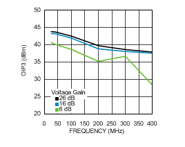 Figure 51. OIP3 vs Frequency
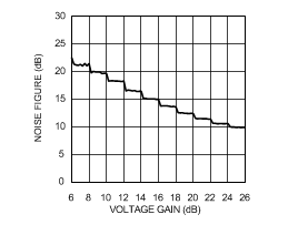 Figure 52. Noise Figure vs Voltage Gain
8.2.2 LMH6882 Used as Twisted Pair Cable Driver
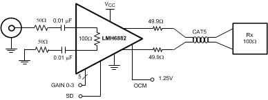 Figure 53. LMH6882 Used as Twisted Pair Cable Driver
8.2.2.1 Design Requirements
Table 11 shows a design example for LMH6882 used as cable driver for driving un-shielded twisted pair (UTP) CAT-5 cables.
Table 11. Example Design Requirement for a Cable Driver
| SPECIFICATION | EXAMPLE DESIGN REQUIREMENT |
|---|---|
| Supply Voltage and Current | 4.75 V to 5.25 V, with a minimum 150-mA supply current |
| Input to Output Device Configuration | Single-ended input to differential output |
| Input frequency range | 0.1 to 100 MHz |
| Voltage Gain Range | 26-dB to 6-dB gain range |
| Output voltage swing | 4 Vppdiff into a 200-Ω load at the output |
| Cable length to be driven | 300 to 400 feet |
8.2.2.2 Detailed Design Procedure
The LMH6882 device can be used as a cable driver to drive (UTP) CAT-5 cable by following these basic procedures:
- Select an appropriate input buffer or drive circuitry to the LMH6882 that provides pre-equalization in the frequency range of interest that needs to be driven down the CAT-5 cable. The cable usually presents attenuation of the signal at the receive end which is proportional to the length of the cable and the frequency being transmitted. In some cases, use of the pre-equalization buffer is not possible which mandates the use of a post-equalizer at the receive end to gain up the received signal.
- Determine the maximum output swing required to be transmitted in-order to receive the signal with good signal integrity. When driving long cable lengths, there is a possibility of corruption of differential signals due to common mode signals which requires the use of devices that offer good common mode rejection. Also, care must be taken to match the source impedance with the characteristic impedance of the CAT-5 cable to minimize signal reflections at higher frequencies. The LMH6882 offers low differential output resistance that makes source matching of driven cable very convenient.
- Verify the electrical and functional compatibility when interfacing LMH6882 digital input pins with the external micro-controller (µC).
- Also, use appropriate power-supply architecture and supply bypass filtering devices to provide stable, low noise supplies as mentioned in the Power Supply Recommendations.
8.2.2.3 Application Curves
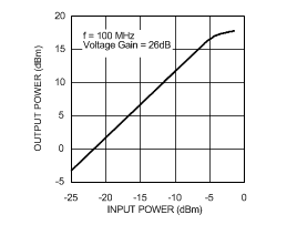 Figure 54. Output Power vs Input Power
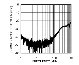 Figure 55. Common Mode Rejection (Sdc21) vs Frequency