SNOSC84D August 2012 – February 2015 LMH6882
PRODUCTION DATA.
- 1 Features
- 2 Applications
- 3 Description
- 4 Revision History
- 5 Pin Configuration and Functions
- 6 Specifications
- 7 Detailed Description
- 8 Application and Implementation
- 9 Power Supply Recommendations
- 10Layout
- 11Device and Documentation Support
- 12Mechanical, Packaging, and Orderable Information
Package Options
Refer to the PDF data sheet for device specific package drawings
Mechanical Data (Package|Pins)
- NJK|36
Thermal pad, mechanical data (Package|Pins)
Orderable Information
5 Pin Configuration and Functions
NJK Package
36-Pins WQFN
Top View
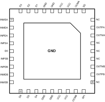
Pin Functions
| PIN | TYPE | DESCRIPTION | |
|---|---|---|---|
| NAME | NO. | ||
| ANALOG I/O | |||
| INPD, INMD | 11, 12, 16, 17 | Analog Input | Differential inputs 100 Ω |
| INPS, INMS | 10, 13, 15, 18 | Analog Input | Single ended inputs 50 Ω |
| OUTP, OUTM | 35, 34, 30, 29 | Analog Output | Differential outputs, low impedance |
| POWER | |||
| GND | 5, 6, 22, 23 | Ground | Ground pins. Connect to low-impedance ground plane. All pin voltages are specified with respect to the voltage on these pins. The exposed thermal pad is internally bonded to the ground pins. |
| VCC | 3, 4, 24, 25 | Power | Power supply pins. Valid power supply range is 4.75 V to 5.25 V. |
| Exposed Center Pad | Thermal/ Ground | Thermal management/ Ground | |
| DIGITAL INPUTS | |||
| SPI | 27 | Digital Input | 0 = Parallel Mode, 1 = Serial Mode |
| PARALLEL MODE DIGITAL PINS, SPI = LOGIC LOW | |||
| D0, D1, D2, D3, D4, D5, D6 | 14, 7, 8, 9, 21, 29, 19 | Digital Input | Attenuator control, D0 = 0.25 dB, D6 = 16 dB |
| SD | 1 | Digital Input | Shutdown 0 = amp on, 1 = amp off |
| SERIAL MODE DIGITAL PINS, SPI = LOGIC HIGH (SPI COMPATIBLE) | |||
| CS | 9 | Digital Input | Chip Select (active low) |
| CLK | 8 | Digital Input | Clock |
| SDO | 14 | Digital Output- Open Emitter | Serial Data Output (Requires external bias.) |
| SDI | 7 | Digital Input | Serial Data In |