SNOSC84D August 2012 – February 2015 LMH6882
PRODUCTION DATA.
- 1 Features
- 2 Applications
- 3 Description
- 4 Revision History
- 5 Pin Configuration and Functions
- 6 Specifications
- 7 Detailed Description
- 8 Application and Implementation
- 9 Power Supply Recommendations
- 10Layout
- 11Device and Documentation Support
- 12Mechanical, Packaging, and Orderable Information
Package Options
Refer to the PDF data sheet for device specific package drawings
Mechanical Data (Package|Pins)
- NJK|36
Thermal pad, mechanical data (Package|Pins)
Orderable Information
10 Layout
10.1 Layout Guidelines
It is very important to employ good high-speed layout techniques when dealing with devices having relatively high gain bandwidth in excess of 1GHz to ensure stability and optimum performance. The LMH6882 evaluation board provides a good reference for suggested layout techniques. The LMH6882 evaluation board was designed for both good signal integrity and thermal dissipation using higher performance (Rogers) dielectric on the top layer. The high performance dielectric provides well matched impedance and low loss to frequencies beyond 1GHz.
TI recommends that the LMH6882 board be multi-layered to improve thermal performance, grounding and power-supply decoupling. The LMH6882 evaluation board is an 8-layered board with the supply sandwiched in-between the GND layers for decoupling and having the stack up as Top layer - GND - GND - GND - Supply - GND - GND - Bottom layer. All signal paths are routed on the top layer on the higher performance (Rogers) dielectric, while the remainder signal layers are conventional FR4.
10.1.1 Uncontrolled Impedance Traces
It is important to pay careful attention while routing high-frequency signal traces on the PCB to maintain signal integrity. A good board layout software package can simplify the trace thickness design to maintain controlled characteristic impedances for high-frequency signals. Eliminating copper (the ground and power plane) from underneath the input and output pins of the device also helps in minimizing parasitic capacitance affecting the high frequency signals near the PCB and package junctions. The LMH6882 evaluation board has copper keep-out areas under both the input and the output traces for this purpose. It is recommended that the application board also follow these keep-out areas to avoid any performance degradation.
10.2 Layout Example
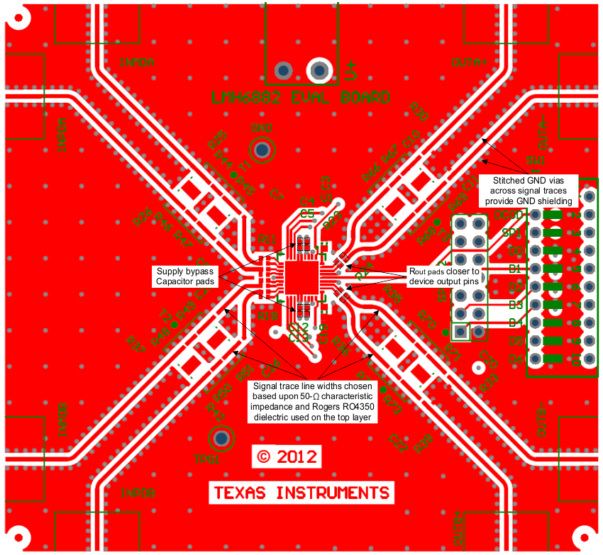 Figure 56. Top Layer
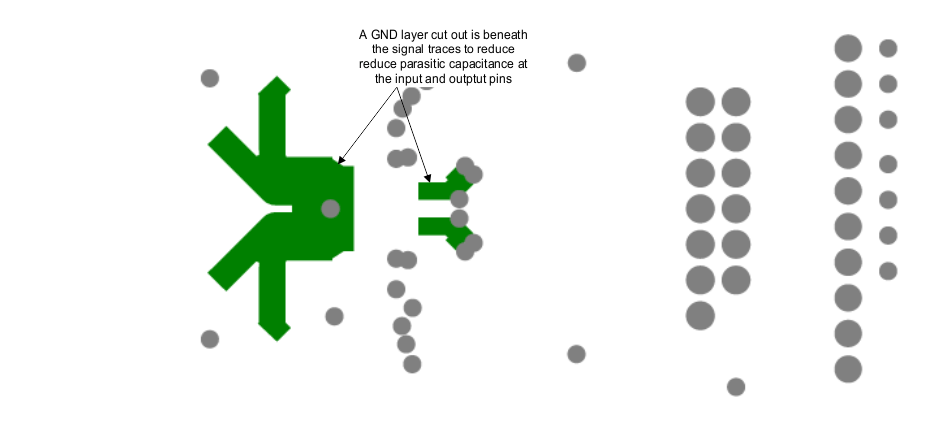 Figure 57. GND Layer
10.3 Thermal Considerations
The LMH6882 is packaged in a thermally enhanced package. The exposed pad on the bottom of the package is the primary means of removing heat from the package. It is recommended, but not necessary, that the exposed pad be connected to the supply ground plane. In any case, the thermal dissipation of the device is largely dependent on the attachment of the exposed pad to the system printed circuit board (PCB). The exposed pad should be attached to as much copper on the PCB as possible, preferably external layers of copper.