SNAS760A April 2018 – January 2022 LMK00334-Q1
PRODUCTION DATA
- 1 Features
- 2 Applications
- 3 Description
- 4 Revision History
- 5 Pin Configuration and Functions
- 6 Specifications
- 7 Parameter Measurement Information
- 8 Detailed Description
- 9 Application and Implementation
- 10Power Supply Recommendations
- 11Layout
- 12Device and Documentation Support
- 13Mechanical, Packaging, and Orderable Information
Package Options
Mechanical Data (Package|Pins)
- RTV|32
Thermal pad, mechanical data (Package|Pins)
- RTV|32
Orderable Information
10.2.1 Power Supply Ripple Rejection
In practical system applications, power supply noise (ripple) can be generated from switching power supplies, digital ASICs or FPGAs, and so forth. While power supply bypassing will help filter out some of this noise, it is important to understand the effect of power supply ripple on the device performance. When a single-tone sinusoidal signal is applied to the power supply of a clock distribution device, such as LMK00334-Q1, it can produce narrow-band phase modulation as well as amplitude modulation on the clock output (carrier). In the single-side band phase noise spectrum, the ripple-induced phase modulation appears as a phase spur level relative to the carrier (measured in dBc).
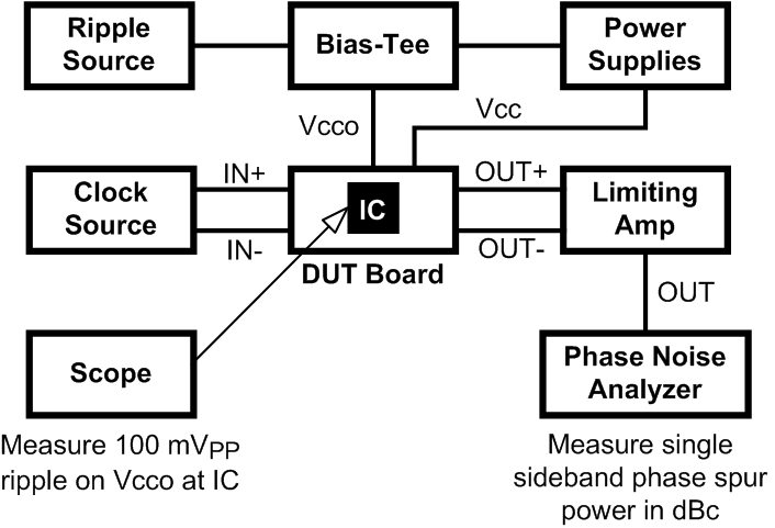
For the LMK00334-Q1, power supply ripple rejection, or PSRR, was measured as the single-sideband phase spur level (in dBc) modulated onto the clock output when a ripple signal was injected onto the VCCO supply. The PSRR test setup is shown in Figure 10-1.
 Figure 10-1 PSRR Test Setup
A signal generator was used to inject a sinusoidal signal onto the VCCO supply of the DUT board, and the peak-to-peak ripple amplitude was measured at the VCCO pins of the device. A limiting amplifier was used to remove amplitude modulation on the differential output clock and convert it to a single-ended signal for the phase noise analyzer. The phase spur level measurements were taken for clock frequencies of 156.25 MHz and 312.5 MHz under the following power supply ripple conditions:
- Ripple amplitude: 100 mVpp on VCCO = 2.5 V
- Ripple frequencies: 100 kHz, 1 MHz, and 10 MHz
Assuming no amplitude modulation effects and small index modulation, the peak-to-peak deterministic jitter (DJ) can be calculated using the measured single-sideband phase spur level (PSRR) as follows:
The PSRR vs. Ripple Frequency plots in Section 6.7 show the ripple-induced phase spur levels at 156.25 MHz and 312.5 MHz. The LMK00334-Q1 exhibits very good and well-behaved PSRR characteristics across the ripple frequency range. The phase spur levels for HCSL are below –72 dBc at 156.25 MHz and below –63 dBc at 312.5 MHz. Using Equation 10, these phase spur levels translate to Deterministic Jitter values of 1.02 ps pk-pk at 156.25 MHz and 1.44 ps pk-pk at 312.5 MHz. Testing has shown that the PSRR performance of the device improves for VCCO = 3.3 V under the same ripple amplitude and frequency conditions.