SNAS489K March 2011 – December 2014 LMK04803 , LMK04805 , LMK04806 , LMK04808
PRODUCTION DATA.
- 1 Features
- 2 Applications
- 3 Description
- 4 Revision History
- 5 Pin Configuration and Functions
- 6 Specifications
-
7 Parameter Measurement Information
- 7.1
Charge Pump Current Specification Definitions
- 7.1.1 Charge Pump Output Current Magnitude Variation Vs. Charge Pump Output Voltage
- 7.1.2 Charge Pump Sink Current Vs. Charge Pump Output Source Current Mismatch
- 7.1.3 Charge Pump Output Current Magnitude Variation vs. Ambient Temperature"Temperature" to "Ambient Temperature" in heading titled "Charge Pump Output Current Magnitude Variation vs. Ambient Temperature"
- 7.2 Differential Voltage Measurement Terminology
- 7.1
Charge Pump Current Specification Definitions
-
8 Detailed Description
- 8.1
Overview
- 8.1.1 System Architecture
- 8.1.2 PLL1 Redundant Reference Inputs (CLKin0/CLKin0* and CLKin1/CLKin1*)
- 8.1.3 PLL1 Tunable Crystal Support
- 8.1.4 VCXO/CRYSTAL Buffered Outputs
- 8.1.5 Frequency Holdover
- 8.1.6 Integrated Loop Filter Poles
- 8.1.7 Internal VCO
- 8.1.8 External VCO Mode
- 8.1.9 Clock Distribution
- 8.1.10 0-Delay
- 8.1.11 Default Startup Clocks
- 8.1.12 Status Pins
- 8.1.13 Register Readback
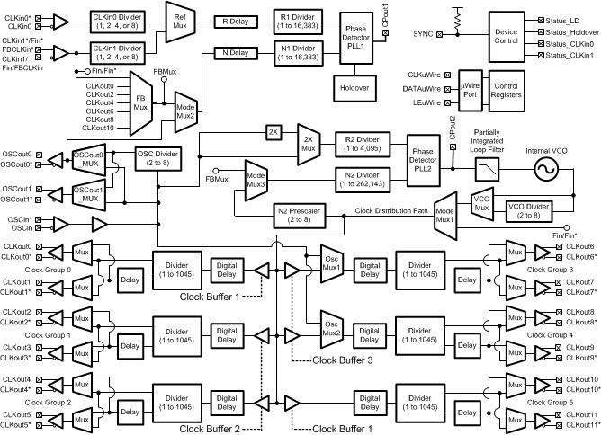
- 8.2 Functional Block Diagram
- 8.3
Feature Description
- 8.3.1 Serial MICROWIRE Timing Diagram
- 8.3.2 Advanced MICROWIRE Timing Diagrams
- 8.3.3 Inputs / Outputs
- 8.3.4 Input Clock Switching
- 8.3.5 Holdover Mode
- 8.3.6 PLLs
- 8.3.7 Status Pins
- 8.3.8 VCO
- 8.3.9
Clock Distribution
- 8.3.9.1 Fixed Digital Delay
- 8.3.9.2 Fixed Digital Delay - Example
- 8.3.9.3
Clock Output Synchronization (SYNC)
- 8.3.9.3.1 Effect of SYNC
- 8.3.9.3.2 Methods of Generating SYNC
- 8.3.9.3.3 Avoiding Clock Output Interruption Due to Sync
- 8.3.9.3.4 SYNC Timing
- 8.3.9.3.5
Dynamically Programming Digital Delay
- 8.3.9.3.5.1 Absolute vs. Relative Dynamic Digital Delay
- 8.3.9.3.5.2 Dynamic Digital Delay and 0-Delay Mode
- 8.3.9.3.5.3 SYNC and Minimum Step Size
- 8.3.9.3.5.4 Programming Overview
- 8.3.9.3.5.5 Internal Dynamic Digital Delay Timing
- 8.3.9.3.5.6 Other Timing Requirements
- 8.3.9.3.5.7 Absolute Dynamic Digital Delay
- 8.3.9.3.5.8 Relative Dynamic Digital Delay
- 8.3.10 0-Delay Mode
- 8.4 Device Functional Modes
- 8.5 Programming
- 8.6
Register Maps
- 8.6.1 Register Map and Readback Register Map
- 8.6.2 Default Device Register Settings After Power On Reset
- 8.6.3
Register Descriptions
- 8.6.3.1
Register R0 TO R5
- 8.6.3.1.1 CLKoutX_Y_PD, Powerdown CLKoutX_Y Output Path
- 8.6.3.1.2 CLKoutX_Y_OSCin_Sel, Clock Group Source
- 8.6.3.1.3 CLKoutY_ADLY_SEL[29], CLKoutX_ADLY_SEL[28], Select Analog Delay
- 8.6.3.1.4 CLKoutX_Y_DDLY, Clock Channel Digital Delay
- 8.6.3.1.5 Reset
- 8.6.3.1.6 POWERDOWN
- 8.6.3.1.7 CLKoutX_Y_HS, Digital Delay Half Shift
- 8.6.3.1.8 CLKoutX_Y_DIV, Clock Output Divide
- 8.6.3.2 Registers R6 TO R8
- 8.6.3.3
Register R10
- 8.6.3.3.1 OSCout1_LVPECL_AMP, LVPECL Output Amplitude Control
- 8.6.3.3.2 OSCout0_TYPE
- 8.6.3.3.3 EN_OSCoutX, OSCout Output Enable
- 8.6.3.3.4 OSCoutX_MUX, Clock Output Mux
- 8.6.3.3.5 PD_OSCin, OSCin Powerdown Control
- 8.6.3.3.6 OSCout_DIV, Oscillator Output Divide
- 8.6.3.3.7 VCO_MUX
- 8.6.3.3.8 EN_FEEDBACK_MUX
- 8.6.3.3.9 VCO_DIV, VCO Divider
- 8.6.3.3.10 FEEDBACK_MUX
- 8.6.3.4 Register R11
- 8.6.3.5 Register R12
- 8.6.3.6 Register R13
- 8.6.3.7 Register 14
- 8.6.3.8 REGISTER 15
- 8.6.3.9 Register 16
- 8.6.3.10 Register 23
- 8.6.3.11
Register 24
- 8.6.3.11.1 PLL2_C4_LF, PLL2 Integrated Loop Filter Component
- 8.6.3.11.2 PLL2_C3_LF, PLL2 Integrated Loop Filter Component
- 8.6.3.11.3 PLL2_R4_LF, PLL2 Integrated Loop Filter Component
- 8.6.3.11.4 PLL2_R3_LF, PLL2 Integrated Loop Filter Component
- 8.6.3.11.5 PLL1_N_DLY
- 8.6.3.11.6 PLL1_R_DLY
- 8.6.3.11.7 PLL1_WND_SIZE
- 8.6.3.12 Register 25
- 8.6.3.13 Register 26
- 8.6.3.14 REGISTER 27
- 8.6.3.15 Register 28
- 8.6.3.16 Register 29
- 8.6.3.17 Register 30
- 8.6.3.18 Register 31
- 8.6.3.1
Register R0 TO R5
- 8.1
Overview
-
9 Application and Implementation
- 9.1
Application Information
- 9.1.1 Loop Filter
- 9.1.2 Driving CLKin and OSCin Inputs
- 9.1.3 Termination and Use of Clock Output (Drivers)
- 9.1.4 Frequency Planning with the LMK0480x Family
- 9.1.5 PLL Programming
- 9.1.6 Digital Lock Detect Frequency Accuracy
- 9.1.7 Calculating Dynamic Digital Delay Values for any Divide
- 9.1.8 Optional Crystal Oscillator Implementation (OSCin/OSCin*)
- 9.1.9 Application Curves
- 9.2 Typical Applications
- 9.3 System Examples
- 9.4 Do's and Don'ts
- 9.1
Application Information
- 10Power Supply Recommendations
- 11Layout
- 12Device and Documentation Support
- 13Mechanical, Packaging, and Orderable Information
Package Options
Mechanical Data (Package|Pins)
- NKD|64
Thermal pad, mechanical data (Package|Pins)
- NKD|64
Orderable Information
8 Detailed Description
8.1 Overview
In default mode of operation, dual PLL mode with internal VCO, the Phase Frequency Detector in PLL1 compares the active CLKinX reference divided by CLKinX_PreR_DIV and PLL1 R divider with the external VCXO or crystal attached to the PLL2 OSCin port divided by PLL1 N divider. The external loop filter for PLL1 should be narrow to provide an ultra clean reference clock from the external VCXO or crystal to the OSCin/OSCin* pins for PLL2.
The Phase Frequency Detector in PLL2 compares the external VCXO or crystal to the internal VCO after the reference and feedback dividers. The VCXO or crystal on the OSCin input is divided by PLL2 R divider. The feedback from the internal VCO is divided by the PLL2 Prescaler, the PLL2 N divider, and optionally the VCO divider.
The bandwidth of the external loop filter for PLL2 should be designed to be wide enough to take advantage of the low in-band phase noise of PLL2 and the low high offset phase noise of the internal VCO. The VCO output is also placed on the distribution path for the Clock Distribution section. The clock distribution consists of 6 groups of dividers and delays which drive 12 outputs. Each clock group allows the user to select a divide value, a digital delay value, and an analog delay. The 6 groups drive programmable output buffers. Two groups allow their input signal to be from the OSCin port directly.
When a 0-delay mode is used, a clock output will be passed through the feedback mux to the PLL1 N Divider for synchronization and 0-delay.
When an external VCO mode is used, the Fin port will be used to input an external VCO signal. PLL2 Phase comparison will now be with this signal divided by the PLL2 N divider and N2 pre-scaler. The VCO divider may not be used. One less clock input is available when using an external VCO mode.
When a single PLL mode is used, PLL1 is powered down. OSCin is used as a reference to PLL2.
8.1.1 System Architecture
The dual loop PLL architecture of the LMK0480x provides the lowest jitter performance over the widest range of output frequencies and phase noise integration bandwidths. The first stage PLL (PLL1) is driven by an external reference clock and uses an external VCXO or tunable crystal to provide a frequency accurate, low phase noise reference clock for the second stage frequency multiplication PLL (PLL2). PLL1 typically uses a narrow loop bandwidth (10 Hz to 200 Hz) to retain the frequency accuracy of the reference clock input signal while at the same time suppressing the higher offset frequency phase noise that the reference clock may have accumulated along its path or from other circuits. This “cleaned” reference clock provides the reference input to PLL2.
The low phase noise reference provided to PLL2 allows PLL2 to operate with a wide loop bandwidth (50 kHz to 200 kHz). The loop bandwidth for PLL2 is chosen to take advantage of the superior high offset frequency phase noise profile of the internal VCO and the good low offset frequency phase noise of the reference VCXO or tunable crystal.
Ultra low jitter is achieved by allowing the external VCXO or crystal’s phase noise to dominate the final output phase noise at low offset frequencies and the internal (or external) VCO’s phase noise to dominate the final output phase noise at high offset frequencies. This results in best overall phase noise and jitter performance.
The LMK0480x allows subsets of the device to be used to increase the flexibility of device. These different modes are selected using MODE: Device Mode. For instance:
- Dual Loop Mode - Typical use case of LMK04808. CLKinX used as reference input to PLL1, OSCin port is connected to VCXO or tunable crystal.
- Single Loop Mode - Powers down PLL1. OSCin port is used as reference input.
- Clock Distribution Mode - Allows input of CLKin1 to be distributed to output with division, digital delay, and analog delay.
See Device Functional Modes for more information on these modes.
8.1.2 PLL1 Redundant Reference Inputs (CLKin0/CLKin0* and CLKin1/CLKin1*)
The LMK0480x has two reference clock inputs for PLL1: CLKin0 and CLKin1. Ref Mux selects CLKin0 or CLKin1. Automatic or manual switching occurs between the inputs.
CLKin0 and CLKin1 each have input dividers. The input divider allows different clock input frequencies to be normalized so that the frequency input to the PLL1 R divider remains constant during automatic switching. By programming these dividers such that the frequency presented to the input of the PLL1_R divider is the same prevents the user from needing to reprogram the PLL1 R divider when the input reference is changed to another CLKin port with a different frequency.
CLKin1 is shared for use as an external 0-delay feedback (FBCLKin), or for use with an external VCO (Fin).
Fast manual switching between reference clocks is possible with external pins Status_CLKin0 and Status_CLKin1.
8.1.3 PLL1 Tunable Crystal Support
The LMK0480x integrates a crystal oscillator on PLL1 for use with an external crystal and varactor diode to perform jitter cleaning.
The LMK0480x must be programmed to enable Crystal mode.
8.1.4 VCXO/CRYSTAL Buffered Outputs
The LMK0480x provides 2 dedicated outputs which are a buffered copy of the PLL2 reference input. This reference input is typically a low noise VCXO or Crystal. When using a VCXO, this output can be used to clock external devices such as microcontrollers, FPGAs, CPLDs, and so forth, before the LMK0480x is programmed.
The OSCout0 buffer output type is programmable to LVDS, LVPECL, or LVCMOS. The OSCout1 buffer is fixed to LVPECL.
The dedicated output buffers OSCout0 and OSCout1 can output frequency lower than the VCXO or Crystal frequency by programming the OSC Divider. The OSC Divider value range is 2 to 8. Each OSCoutX can individually choose to use the OSC Divider output or to bypass the OSC Divider.
Two clock output groups can also be programmed to be driven by OSCin. This allows a total of 4 additional differential outputs to be buffered outputs of OSCin. When programmed in this way, a total of 6 differential outputs can be driven by a buffered copy of OSCin.
VCXO/Crystal buffered outputs cannot be synchronized to the VCO clock distribution outputs. The assertion of SYNC will still cause these outputs to become low temporarily. Since these outputs will turn off and on asynchronously with respect to the VCO sourced clock outputs during a SYNC, it is possible for glitches to occur on the buffered clock outputs when SYNC is asserted and unasserted. If the NO_SYNC_CLKoutX_Y bits are set these outputs will not be affected by the SYNC event except that the phase relationship will change with the other synchronized clocks unless a buffered clock output is used as a qualification clock during SYNC.
8.1.5 Frequency Holdover
The LMK0480x supports holdover operation to keep the clock outputs on frequency with minimum drift when the reference is lost until a valid reference clock signal is re-established.
8.1.6 Integrated Loop Filter Poles
The LMK0480x features programmable 3rd and 4th order loop filter poles for PLL2. These internal resistors and capacitor values may be selected from a fixed range of values to achieve either a 3rd or 4th order loop filter response. The integrated programmable resistors and capacitors compliment external components mounted near the chip.
These integrated components can be effectively disabled by programming the integrated resistors and capacitors to their minimum values.
8.1.7 Internal VCO
The output of the internal VCO is routed to a mux which allows the user to select either the direct VCO output or a divided version of the VCO for the Clock Distribution Path. This same selection is also fed back to the PLL2 phase detector through a prescaler and N-divider.
The mux selectable VCO divider has a divide range of 2 to 8 with 50% output duty cycle for both even and odd divide values.
The primary use of the VCO divider is to achieve divides greater than the clock output divider supports alone.
8.1.8 External VCO Mode
The Fin/Fin* input allows an external VCO to be used with PLL2 of the LMK0480x.
Using an external VCO reduces the number of available clock inputs by one.
8.1.9 Clock Distribution
The LMK0480x features a total of 12 outputs driven from the internal or external VCO.
All VCO driven outputs have programmable output types. They can be programmed to LVPECL, LVDS, or LVCMOS. When all distribution outputs are configured for LVCMOS or single ended LVPECL a total of 24 outputs are available.
If the buffered OSCin outputs OSCout0 and OSCout1 are included in the total number of clock outputs the LMK0480x is able to distribute, then up to 14 differential clocks or up to 28 single ended clocks may be generated with the LMK0480x.
The following sections discuss specific features of the clock distribution channels that allow the user to control various aspects of the output clocks.
8.1.9.1 CLKout DIVIDER
Each clock group, which is a pair of outputs such as CLKout0 and CLKout1, has a single clock output divider. The divider supports a divide range of 1 to 1045 (even and odd) with 50% output duty cycle. When divides of 26 or greater are used, the divider/delay block uses extended mode.
The VCO Divider may be used to reduce the divide needed by the clock group divider so that it may operate in normal mode instead of extended mode. This can result in a small current saving if enabling the VCO Divider allows 3 or more clock output divides to change from extended to normal mode.
8.1.9.2 CLKout Delay
See Clock Distribution section for details on both a fine (analog) and coarse (digital) delay for phase adjustment of the clock outputs.
The fine (analog) delay allows a nominal 25 ps step size and range from 0 to 475 ps of total delay. Enabling the analog delay adds a nominal 500 ps of delay in addition to the programmed value. When adjusting analog delay, glitches may occur on the clock outputs being adjusted. Analog delay may not operate at frequencies above the minimum-ensured maximum output frequency of 1536 MHz.
The coarse (digital) delay allows a group of outputs to be delayed by 4.5 to 12 clock distribution path cycles in normal mode, or from 12.5 to 522 VCO cycles in extended mode. The delay step can be as small as half the period of the clock distribution path by using the CLKoutX_Y_HS bit provided the output divide value is greater than 1. For example, a 2-GHz VCO frequency without the use of the VCO divider results in 250 ps coarse tuning steps.. The coarse (digital) delay value takes effect on the clock outputs after a SYNC event.
There are 3 different ways to use the digital (coarse) delay:
These are further discussed in Clock Distribution.
8.1.9.3 Programmable Output Type
For increased flexibility all LMK0480x clock outputs (CLKoutX) and OSCout0 can be programmed to an LVDS, LVPECL, or LVCMOS output type. OSCout1 is fixed as LVPECL.
Any LVPECL output type can be programmed to 700, 1200, 1600, or 2000 mVpp amplitude levels. The 2000 mVpp LVPECL output type is a Texas Instruments proprietary configuration that produces a 2000 mVpp differential swing for compatibility with many data converters and is also known as 2VPECL.
8.1.9.4 Clock Output Synchronization
Using the SYNC input causes all active clock outputs to share a rising edge. See Clock Output Synchronization (SYNC) for more information.
The SYNC event also causes the digital delay values to take effect.
8.1.10 0-Delay
The 0-delay mode synchronizes the input clock phase to the output clock phase. The 0-delay feedback may be performed with an internal feedback loop from any of the clock groups or with an external feedback loop into the FBCLKin port as selected by the FEEDBACK_MUX.
Without using 0-delay mode there will be D possible fixed phase relationships from clock input to clock output depending on the clock output divide value.
Using an external 0-delay feedback reduces the number of available clock inputs by one.
8.1.11 Default Startup Clocks
Before the LMK0480x is programmed, CLKout8 is enabled and operating at a nominal frequency and CLKout6 and OSCout0 are enabled and operating at the OSCin frequency. These clocks can be used to clock external devices such as microcontrollers, FPGAs, CPLDs, and so forth, before the LMK0480x is programmed.
For CLKout6 and OSCout0 to work before the LMK0480x is programmed, the device must not be using Crystal mode.
8.1.12 Status Pins
The LMK0480x provides status pins which can be monitored for feedback or in some cases used for input depending upon device programming. For example:
- The Status_Holdover pin may indicate if the device is in hold-over mode.
- The Status_CLKin0 pin may indicate the LOS (loss-of-signal) for CLKin0.
- The Status_CLKin0 pin may be an input for selecting the active clock input.
- The Status_LD pin may indicate if the device is locked.
The status pins can be programmed to a variety of other outputs including analog lock detect, PLL divider outputs, combined PLL lock detect signals, PLL1 Vtune railing, readback, and so forth. Refer to the Programming of this datasheet for more information. Default pin programming is captured in Table 18.
8.1.13 Register Readback
Programmed registers may be read back using the MICROWIRE interface. For readback, one of the status pins must be programmed for readback mode.
At no time may registers be programed to values other than the valid states defined in the datasheet.
8.2 Functional Block Diagram
8.3 Feature Description
8.3.1 Serial MICROWIRE Timing Diagram
For timing specifications, see Timing Requirements. Register programming information on the DATAuWire pin is clocked into a shift register on each rising edge of the CLKuWire signal. On the rising edge of the LEuWire signal, the register is sent from the shift register to the register addressed. A slew rate of at least 30 V/µs is recommended for these signals. After programming is complete the CLKuWire, DATAuWire, and LEuWire signals should be returned to a low state. If the CLKuWire or DATAuWire lines are toggled while the VCO is in lock, as is sometimes the case when these lines are shared with other parts, the phase noise may be degraded during this programming.
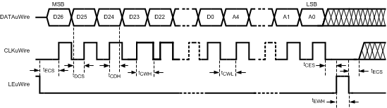 Figure 6. MICROWIRE Input Timing Diagram
8.3.2 Advanced MICROWIRE Timing Diagrams
8.3.2.1 Three Extra Clocks or Double Program
For timing specifications, see Timing Requirements. Figure 7 shows the timing for the programming sequence for loading CLKoutX_Y_DIV > 25 or CLKoutX_Y_DDLY > 12 as described in Special Programming Case for R0 to R5 for CLKoutX_Y_DIV and CLKoutX_Y_DDLY.
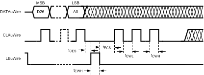 Figure 7. MICROWIRE Timing Diagram: Extra CLKuWire Pulses for R0 to R5
8.3.2.2 Three Extra Clocks with LEuWire High
For timing specifications, see Timing Requirements. Figure 8 shows the timing for the programming sequence which allows SYNC_EN_AUTO = 1 when loading CLKoutX_Y_DIV > 25 or CLKoutX_Y_DDLY > 12. When SYNC_EN_AUTO = 1, a SYNC event is automatically generated on the falling edge of LEuWire. See Special Programming Case for R0 to R5 for CLKoutX_Y_DIV and CLKoutX_Y_DDLY.
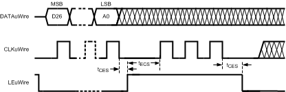 Figure 8. MICROWIRE Timing Diagram: Extra CLKuWire Pulses for R0 to R5 with LEuWire Asserted
8.3.2.3 Readback
For timing specifications, see Timing Requirements. See Readback for more information on performing a readback operation. Figure 9 shows timing for LEuWire for both READBACK_LE = 1 and 0.
The rising edges of CLKuWire during MICROWIRE readback continue to clock data on DATAuWire into the device during readback. If after the readback, LEuWire transitions from low to high, this data will be latched to the decoded register. The decoded register address consists of the last 5 bits clocked on DATAuWire as shown in Figure 9.
 Figure 9. MICROWIRE Readback Timing Diagram
8.3.3 Inputs / Outputs
8.3.3.1 PLL1 Reference Inputs (CLKin0 and CLKin1)
The reference clock inputs for PLL1 may be selected from either CLKin0 or CLKin1. The user has the capability to manually select one of the inputs or to configure an automatic switching mode of operation. See Input Clock Switching for more info.
CLKin0 and CLKin1 have dividers which allow the device to switch between reference inputs of different frequencies automatically without needing to reprogram the PLL1 R divider. The CLKin pre-divider values are 1, 2, 4, and 8.
CLKin1 input can alternatively be used for external feedback in 0-delay mode (FBCLKin) or for an external VCO input port (Fin).
8.3.3.2 PLL2 OSCin / OSCin* Port
The feedback from the external oscillator being locked with PLL1 drives the OSCin/OSCin* pins. Internally this signal is routed to the PLL1 N Divider and to the reference input for PLL2.
This input may be driven with either a single-ended or differential signal and must be AC coupled. If operated in single ended mode, the unused input must be connected to GND with a 0.1 µF capacitor.
8.3.3.3 Crystal Oscillator
The internal circuitry of the OSCin port also supports the optional implementation of a crystal based oscillator circuit. A crystal, a varactor diode, and a small number of other external components may be used to implement the oscillator. The internal oscillator circuit is enabled by setting the EN_PLL2_XTAL bit. See EN_PLL2_XTAL.
8.3.4 Input Clock Switching
Manual, pin select, and automatic are three different kinds clock input switching modes can be set with the CLKin_SELECT_MODE register.
Below is information about how the active input clock is selected and what causes a switching event in the various clock input selection modes.
8.3.4.1 Input Clock Switching - Manual Mode
When CLKin_SELECT_MODE is 0 or 1 then CLKin0 or CLKin1 respectively is always selected as the active input clock. Manual mode will also override the EN_CLKinX bits such that the CLKinX buffer will operate even if CLKinX is disabled with EN_CLKinX = 0.
- Entering Holdover: If holdover mode is enabled, then holdover mode is entered if Digital lock detect of PLL1 goes low and DISABLE_DLD1_DET = 0.
- Exiting Holdover: The active clock for automatic exit of holdover mode is the manually selected clock input.
8.3.4.2 Input Clock Switching - Pin Select Mode
When CLKin_SELECT_MODE is 3, the pins Status_CLKin0 and Status_CLKin1 select which clock input is active.
- Clock Switch Event: Pins: Changing the state of Status_CLKin0 or Status_CLKin1 pins causes an input clock switch event.
- Clock Switch Event: PLL1 DLD: To prevent PLL1 DLD high to low transition from causing a input clock switch event and causing the device to enter holdover mode, disable the PLL1 DLD detect by setting DISABLE_DLD1_DET = 1. This is the preferred behavior for Pin Select Mode.
-
Configuring Pin Select Mode:
- The Status_CLKin0_TYPE must be programmed to an input value for the Status_CLKin0 pin to function as an input for pin select mode.
- The Status_CLKin1_TYPE must be programmed to an input value for the Status_CLKin1 pin to function as an input for pin select mode.
- If the Status_CLKinX_TYPE is set as output, the input value is considered 0.
- The polarity of Status_CLKin1 and Status_CLKin0 input pins cannot be inverted with the CLKin_SEL_INV bit.
- Table 1 defines which input clock is active depending on Status_CLKin0 and Status_CLKin1 state.
Table 1. Active Clock Input - Pin Select Mode
| STATUS_CLKin1 | STATUS_CLKin0 | ACTIVE CLOCK |
|---|---|---|
| 0 | 0 | CLKin0 |
| 0 | 1 | CLKin1 |
| 1 | 0 | Reserved |
| 1 | 1 | Holdover |
The pin select mode will override the EN_CLKinX bits such that the CLKinX buffer will operate even if CLKinX is disabled with EN_CLKinX = 0. To switch as fast as possible, keep the clock input buffers enabled (EN_CLKinX = 1) that could be switched to.
8.3.4.2.1 Pin Select Mode and Host
When in the pin select mode, the host can monitor conditions of the clocking system which could cause the host to switch the active clock input. The LMK0480x device can also provide indicators on the Status_LD and Status_HOLDOVER like "DAC Rail," "PLL1 DLD", "PLL1 and PLL2 DLD" which the host can use in determining which clock input to use as active clock input.
8.3.4.2.2 Switch Event without Holdover
When an input clock switch event is triggered and holdover mode is disabled, the active clock input immediately switches to the selected clock. When PLL1 is designed with a narrow loop bandwidth, the switching transient is minimized.
8.3.4.2.3 Switch Event with Holdover
When an input clock switch event is triggered and holdover mode is enabled, the device will enter holdover mode and remain in holdover until a holdover exit condition is met as described in Holdover Mode. Then the device will complete the reference switch to the pin selected clock input.
8.3.4.3 Input Clock Switching - Automatic Mode
When CLKin_SELECT_MODE is 4, the active clock is selected in priority order of enabled clock inputs starting upon an input clock switch event. The priority order of the clocks is CLKin0 → CLKin1 → CLKin0, and so forth.
For a clock input to be eligible to be switched through, it must be enabled using EN_CLKinX.
8.3.4.3.1 Starting Active Clock
Upon programming this mode, the currently active clock remains active if PLL1 lock detect is high. To ensure a particular clock input is the active clock when starting this mode, program CLKin_SELECT_MODE to the manual mode which selects the desired clock input (CLKin0 or 1). Wait for PLL1 to lock PLL1_DLD = 1, then select this mode with CLKin_SELECT_MODE = 4.
8.3.4.3.2 Clock Switch Event: PLL1 DLD
A loss of lock as indicated by PLL1’s DLD signal (PLL1_DLD = 0) will cause an input clock switch event if DISABLE_DLD1_DET = 0. PLL1 DLD must go high (PLL1_DLD = 1) in between input clock switching events.
8.3.4.3.3 Clock Switch Event: PLL1 Vtune Rail
If Vtune_RAIL_DET_EN is set and the PLL1 Vtune voltage crosses the DAC high or low threshold, holdover mode will be entered. Since PLL1_DLD = 0 in holdover a clock input switching event will occur.
8.3.4.3.4 Clock Switch Event with Holdover
Clock switch event with holdover enabled is recommended in this input clock switching mode. When an input clock switch event occurs, holdover mode is entered and the active clock is set to the clock input defined by the Status_CLKinX pins. When the new active clock meets the holdover exit conditions, holdover is exited and the active clock will continue to be used as a reference until another input clock switch event. PLL1 DLD must go high in between input clock switching events.
8.3.4.4 Input Clock Switching - Automatic Mode with Pin Select
When CLKin_SELECT_MODE is 6, the active clock is selected using the Status_CLKinX pins upon an input clock switch event according to Table 2.
8.3.4.4.1 Starting Active Clock
Upon programming this mode, the currently active clock remains active if PLL1 lock detect is high. To ensure a particular clock input is the active clock when starting this mode, program CLKin_SELECT_MODE to the manual mode which selects the desired clock input (CLKin0 or 1). Wait for PLL1 to lock PLL1_DLD = 1, then select this mode with CLKin_SELECT_MODE = 6.
8.3.4.4.2 Clock Switch Event: PLL1 DLD
An input clock switch event is generated by a loss of lock as indicated by PLL1's DLD signal (PLL1 DLD = 0).
8.3.4.4.3 Clock Switch Event: PLL1 Vtune Rail
If Vtune_RAIL_DET_EN is set and the PLL1 Vtune voltage crosses the DAC threshold, holdover mode will be entered. Since PLL1_DLD = 0 in holdover, a clock input switching event will occur.
8.3.4.4.4 Clock Switch Event with Holdover
Clock switch event with holdover enabled is recommended in this input clock switching mode. When an input clock switch event occurs, holdover mode is entered and the active clock is set to the clock input defined by the Status_CLKinX pins. When the new active clock meets the holdover exit conditions, holdover is exited and the active clock will continue to be used as a reference until another input clock switch event. PLL1 DLD must go high in between input clock switching events."
Table 2. Active Clock Input - Auto Pin Mode
| STATUS_CLKin1(1) | STATUS_CLKin0 | ACTIVE CLOCK |
|---|---|---|
| X | 1 | CLKin0 |
| 1 | 0 | CLKin1 |
| 0 | 0 | Reserved |
8.3.5 Holdover Mode
Holdover mode causes PLL2 to stay locked on frequency with minimal frequency drift when an input clock reference to PLL1 becomes invalid. While in holdover mode, the PLL1 charge pump is TRI-STATED and a fixed tuning voltage is set on CPout1 to operate PLL1 in open loop.
8.3.5.1 Enable Holdover
Program HOLDOVER_MODE to enable holdover mode. Holdover mode can be manually enabled by programming the FORCE_HOLDOVER bit.
The holdover mode can be set to operate in 2 different sub-modes.
- Fixed CPout1 (EN_TRACK = 0 or 1, EN_MAN_DAC = 1).
- Tracked CPout1 (EN_TRACK = 1, EN_MAN_DAC = 0).
- Not valid when EN_VTUNE_RAIL_DET = 1.
Updates to the DAC value for the Tracked CPout1 sub-mode occurs at the rate of the PLL1 phase detector frequency divided by DAC_CLK_DIV. These updates occur any time EN_TRACK = 1.
The DAC update rate should be programmed for <= 100 kHz to ensure DAC holdover accuracy.
When tracking is enabled the current voltage of DAC can be readback, see DAC_CNT.
8.3.5.2 Entering Holdover
The holdover mode is entered as described in Input Clock Switching. Typically this is because:
- FORCE_HOLDOVER bit is set.
- PLL1 loses lock according to PLL1_DLD, and
- HOLDOVER_MODE = 2
- DISABLE_DLD1_DET = 0
- CPout1 voltage crosses DAC high or low threshold, and
- HOLDOVER_MODE = 2
- EN_VTUNE_RAIL_DET = 1
- EN_TRACK = 1
- DAC_HIGH_TRIP = User Value
- DAC_LOW_TRIP = User Value
- EN_MAN_DAC = 1
- MAN_DAC = User Value
8.3.5.3 During Holdover
PLL1 is run in open loop mode.
- PLL1 charge pump is set to TRI-STATE.
- PLL1 DLD will be unasserted.
- The HOLDOVER status is asserted
- During holdover If PLL2 was locked prior to entry of holdover mode, PLL2 DLD will continue to be asserted.
- CPout1 voltage will be set to:
- a voltage set in the MAN_DAC register (fixed CPout1).
- a voltage determined to be the last valid CPout1 voltage (tracked CPout1).
- PLL1 DLD will attempt to lock with the active clock input.
The HOLDOVER status signal can be monitored on the Status_HOLDOVER or Status_LD pin by programming the HOLDOVER_MUX or LD_MUX register to "Holdover Status."
8.3.5.4 Exiting Holdover
Holdover mode can be exited in one of two ways.
- Manually, by programming the device from the host.
- Automatically, By a clock operating within a specified ppm of the current PLL1 frequency on the active clock input. See Input Clock Switching for more detail on which clock input is active.
To exit holdover by programming, set HOLDOVER_MODE = Disabled. HOLDOVER_MODE can then be re-enabled by programming HOLDOVER_MODE = Enabled. Care should be taken to ensure that the active clock upon exiting holdover is as expected, otherwise the CLKin_SELECT_MODE register may need to be re-programmed.
8.3.5.5 Holdover Frequency Accuracy and DAC Performance
When in holdover mode PLL1 will run in open loop and the DAC will set the CPout1 voltage. If Fixed CPout1 mode is used, then the output of the DAC will be a voltage dependant upon the MAN_DAC register. If Tracked CPout1 mode is used, then the output of the DAC will be the voltage at the CPout1 pin before holdover mode was entered. When using Tracked mode and EN_MAN_DAC = 1, during holdover the DAC value is loaded with the programmed value in MAN_DAC, not the tracked value.
When in Tracked CPout1 mode the DAC has a worst case tracking error of ±2 LSBs once PLL1 tuning voltage is acquired. The step size is approximately 3.2 mV, therefore the VCXO frequency error during holdover mode caused by the DAC tracking accuracy is ±6.4 mV × Kv, where Kv is the tuning sensitivity of the VCXO in use. Therefore the accuracy of the system when in holdover mode in ppm is:
Example: consider a system with a 19.2-MHz clock input, a 153.6-MHz VCXO with a Kv of 17 kHz/V. The accuracy of the system in holdover in ppm is:
It is important to account for this frequency error when determining the allowable frequency error window to cause holdover mode to exit.
8.3.5.6 Holdover Mode - Automatic Exit of Holdover
The LMK0480x device can be programmed to automatically exit holdover mode when the accuracy of the frequency on the active clock input achieves a specified accuracy. The programmable variables include PLL1_WND_SIZE and DLD_HOLD_CNT.
See Digital Lock Detect Frequency Accuracy to calculate the register values to cause holdover to automatically exit upon reference signal recovery to within a user specified ppm error of the holdover frequency.
It is possible for the time to exit holdover to vary because the condition for automatic holdover exit is for the reference and feedback signals to have a time/phase error less than a programmable value. Because it is possible for two clock signals to be very close in frequency but not close in phase, it may take a long time for the phases of the clocks to align themselves within the allowable time/phase error before holdover exits.
8.3.6 PLLs
8.3.6.1 PLL1
The maximum phase detector frequency (fPD1) of PLL1 is 40 MHz. Since a narrow loop bandwidth should be used for PLL1, the need to operate at high phase detector rate to lower the in-band phase noise becomes unnecessary. The maximum values for the PLL1 R and N dividers is 16,383. Charge pump current ranges from 100 to 1600 µA. PLL1 N divider may be driven by OSCin port at the OSCout0_MUX output (default) or by internal or external feedback as selected by Feedback Mux in 0-delay mode.
Low charge pump currents and phase detector frequencies aid design of low loop bandwidth loop filters with reasonably sized components to allow the VCXO or PLL2 to dominate phase noise inside of PLL2 loop bandwidth. High charge pump currents may be used by PLL1 when using VCXOs with leaky tuning voltage inputs to improve system performance.
8.3.6.2 PLL2
PLL2's maximum phase detector frequency (fPD2) is 155 MHz. Operating at highest possible phase detector rate will ensure low in-band phase noise for PLL2 which in turn produces lower total jitter. The in-band phase noise from the reference input and PLL is proportional to N2. The maximum value for the PLL2 R divider is 4,095. The maximum value for the PLL2 N divider is 262,143. The N2 Prescaler in the total N feedback path can be programmed for values 2 to 8 (all divides even and odd). Charge pump current ranges from 100 to 3200 µA.
High charge pump currents help to widen the PLL2 loop bandwidth to optimize PLL2 performance.
8.3.6.2.1 PLL2 Frequency Doubler
The PLL2 reference input at the OSCin port may be routed through a frequency doubler before the PLL2 R Divider. The frequency doubler feature allows the phase comparison frequency to be increased when a relatively low frequency oscillator is driving the OSCin port. By doubling the PLL2 phase detector frequency, the in-band PLL2 noise is reduced by about 3 dB.
When using the doubler, PLL2 R Divider may be used to reduce the phase detector frequency to the limit of the PLL2 maximum phase detector frequency.
For applications in which the OSCin frequency and PLL2 phase detector frequency are equal, the best PLL2 in-band noise can be achieved when the doubler is enabled (EN_PLL2_REF_2X = 1) and the PLL2 R divide value is 2. Do not use doubler disabled (EN_PLL2_REF_2X = 0) and PLL2 R divide value of 1.
8.3.6.3 Digital Lock Detect
Both PLL1 and PLL2 support digital lock detect. Digital lock detect compares the phase between the reference path (R) and the feedback path (N) of the PLL. When the time error, which is phase error, between the two signals is less than a specified window size (ε) a lock detect count increments. When the lock detect count reaches a user specified value lock detect is asserted true. Once digital lock detect is true, a single phase comparison outside the specified window will cause digital lock detect to be asserted false. This is illustrated in Figure 10.
The incremental lock detect count feature functions as a digital filter to ensure that lock detect isn't asserted for only a brief time when the phases of R and N are within the specified tolerance for only a brief time during initial phase lock.
The digital lock detect signal can be monitored on the Status_LD or Status_Holdover pin. The pin may be programmed to output the status of lock detect for PLL1, PLL2, or both PLL1 and PLL2.
See Digital Lock Detect Frequency Accuracy for more detailed information on programming the registers to achieve a specified frequency accuracy in ppm with lock detect.
The digital lock detect feature can also be used with holdover to automatically exit holdover mode. See Holdover Mode for more info.
 Figure 10. Digital Lock Detect Flowchart
8.3.7 Status Pins
The Status_LD, Status_HOLDOVER, Status_CLKin0, Status_CLKin1, and SYNC pins can be programmed to output a variety of signals for indicating various statuses like digital lock detect, holdover, several DAC indicators, and several PLL divider outputs.
8.3.7.1 Logic Low
This is a vary simple output. In combination with the output _MUX register, this output can be toggled between high and low. Useful to confirm MICROWIRE programming or as a general purpose IO.
8.3.7.2 Digital Lock Detect
PLL1 DLD, PLL2 DLD, and PLL1 + PLL2 are selectable on certain output pins. See Digital Lock Detect for more information.
8.3.7.3 Holdover Status
Indicates if the device is in Holdover mode. See HOLDOVER_MODE for more information.
8.3.7.4 DAC
Various flags for the DAC can be monitored including DAC Locked, DAC Rail, DAC Low, and DAC High.
When the PLL1 tuning voltage crosses the low threshold, DAC Low is asserted. When PLL1 tuning voltage crosses the high threshold, DAC High is asserted. When either DAC Low or DAC High is asserted, DAC Rail will also be asserted.
DAC Locked is asserted when EN_Track = 1 and DAC is closely tracking the PLL1 tuning voltage.
8.3.7.5 PLL Divider Outputs
The PLL divider outputs are useful for debugging failure to lock issues. It allows the user to measure the frequency the PLL inputs are receiving. The settings of PLL1_R, PLL1_N, PLL2_R, and PLL2_N output pulses at the phase detector rate. The settings of PLL1_R / 2, PLL1_N / 2, PLL2_R / 2, and PLL2_N / 2 output a 50% duty cycle waveform at half the phase detector rate.
8.3.7.6 CLKinX_LOS
The clock input loss of signal indicator is asserted when LOS is enabled (EN_LOS) and the clock no longer detects an input as defined by the time-out threshold, LOS_TIMEOUT.
8.3.7.7 CLKinX Selected
If this clock is the currently selected/active clock, this pin will be asserted.
8.3.7.8 MICROWIRE Readback
The readback data can be output on any pin programmable to readback mode. For more information on readback see Readback.
8.3.8 VCO
The integrated VCO uses a frequency calibration routine when register R30 is programmed to lock VCO to target frequency. Register R30 contains the PLL2_N register.
During the frequency calibration the PLL2_N_CAL value is used instead of PLL2_N, this allows 0-delay modes to have a separate PLL2 N value for VCO frequency calibration and regular operation. See Register 29, Register 30, and PLL Programming for more information.
8.3.9 Clock Distribution
8.3.9.1 Fixed Digital Delay
This section discussing Fixed Digital delay and associated registers is fundamental to understanding digital delay and dynamic digital delay.
Clock outputs may be delayed or advanced from one another by up to 517.5 clock distribution path periods. By programming a digital delay value from 4.5 to 522 clock distribution path periods, a relative clock output delay from 0 to 517.5 periods is achieved. The CLKoutX_Y_DDLY (5 to 522) and CLKoutX_Y_HS (-0.5 or 0) registers set the digital delay as shown in Table 3.
Table 3. Possible Digital Delay Values
| CLKoutX_Y_DDLY | CLKoutX_Y_HS | DIGITAL DELAY |
|---|---|---|
| 5 | 1 | 4.5 |
| 5 | 0 | 5 |
| 6 | 1 | 5.5 |
| 6 | 0 | 6 |
| 7 | 1 | 6.5 |
| 7 | 0 | 7 |
| ... | ... | ... |
| 520 | 0 | 520 |
| 521 | 1 | 520.5 |
| 521 | 0 | 521 |
| 522 | 1 | 521.5 |
| 522 | 0 | 522 |
Note: Digital delay values only take effect during a SYNC event and if the NO_SYNC_CLKoutX_Y bit is cleared for this clock group. See Clock Output Synchronization (SYNC) for more information.
The resolution of digital delay is determined by the frequency of the clock distribution path. The clock distribution path is the output of Mode Mux1 (Functional Block Diagram). The best resolution of digital delay is achieved by bypassing the VCO divider.
The digital delay between clock outputs can be dynamically adjusted with no or minimum disruption of the output clocks. See Dynamically Programming Digital Delay for more information.
8.3.9.2 Fixed Digital Delay - Example
Given a VCO frequency of 2949.12 MHz and no VCO divider, by using digital delay the outputs can be adjusted in 1 / (2 * 2949.12 MHz) = ~169.54 ps steps.
To achieve quadrature (90 degree shift) between the 122.88-MHz outputs on CLKout4 and CLKout6 from a VCO frequency of 2949.12 MHz and bypassing the VCO divider, consider the following:
- The frequency of 122.88 MHz has a period of ~8.14 ns.
- To delay 90 degrees of a 122.88-MHz clock period requires a ~2.03 ns delay.
- Given a digital delay step of ~169.54 ps, this requires a digital delay value of 12 steps (2.03 ns / 169.54 ps = 12).
- Since the 12 steps are half period steps, CLKout6_7_DDLY is programmed 6 full periods beyond 5 for a total of 11.
This result in the following programming:
- Clock output dividers to 24. CLKout4_5_DIV = 24 and CLKout6_7_DIV = 24.
- Set first clock digital delay value. CLKout4_5_DDLY = 5, CLKout4_5_HS = 0.
- Set second 90 degree shifted clock digital delay value. CLKout6_7_DDLY = 11, CLKout6_7_HS = 0.
Table 4 shows some of the possible phase delays in degrees achievable in the above example.
Table 4. Relative Phase Shift from CLKout4 and 5 to CLKout6 and 7(1)
| CLKout6_7_DDLY | CLKout6_7_HS | RELATIVE DIGITAL DELAY | DEGREES of 122.88 MHz |
|---|---|---|---|
| 5 | 1 | -0.5 | -7.5° |
| 5 | 0 | 0.0 | 0° |
| 6 | 1 | 0.5 | 7.5° |
| 6 | 0 | 1.0 | 15.0° |
| 7 | 1 | 1.5 | 22.5° |
| 7 | 0 | 2.0 | 30.0° |
| 8 | 1 | 2.5 | 37.5° |
| 8 | 0 | 3.0 | 45.0° |
| 9 | 1 | 3.5 | 52.5° |
| 9 | 0 | 4.0 | 60.0° |
| 10 | 1 | 4.5 | 67.5° |
| 10 | 0 | 5.0 | 75.0° |
| 11 | 1 | 5.5 | 82.5° |
| 11 | 0 | 6.0 | 90.0° |
| 12 | 1 | 6.5 | 97.5° |
| 12 | 0 | 7.0 | 105.0° |
| 13 | 1 | 7.5 | 112.5° |
| 13 | 0 | 8.0 | 120.0° |
| 14 | 1 | 8.5 | 127.5° |
| ... | ... | ... | ... |
Figure 12 illustrates clock outputs programmed with different digital delay values during a SYNC event.
Refer to Dynamically Programming Digital Delay for more information on dynamically adjusting digital delay.
8.3.9.3 Clock Output Synchronization (SYNC)
The purpose of the SYNC function is to synchronize the clock outputs with a fixed and known phase relationship between each clock output selected for SYNC. SYNC can also be used to hold the outputs in a low or 0 state. The NO_SYNC_CLKoutX_Y bits can be set to disable synchronization for a clock group.
To enable SYNC, EN_SYNC must be set. See EN_SYNC, Enable Synchronization.
The digital delay value set by CLKoutX_Y_DDLY takes effect only upon a SYNC event. The digital delay due to CLKoutX_Y_HS takes effect immediately upon programming. See Dynamically Programming Digital Delay for more information on dynamically changing digital delay.
During a SYNC event, clock outputs driven by the VCO are not synchronized to clock outputs driven by OSCin. OSCout0 and OSCout1 are always driven by OSCin. CLKout6, 7, 8, or 9 may be driven by OSCin depending on the CLKoutX_Y_OSCin_Sel bit value. While SYNC is asserted, NO_SYNC_CLKoutX_Y operates normally for CLKout6, 7, 8, and 9 under all circumstances. SYNC operates normally for CLKout6, 7, 8, and 9 when driven by VCO.
8.3.9.3.1 Effect of SYNC
When SYNC is asserted, the outputs to be synchronized are held in a logic low state. When SYNC is unasserted, the clock outputs to be synchronized are activated and will transition to a high state simultaneously with one another except where different digital delay values have been programmed.
Refer to Dynamically Programming Digital Delay for SYNC functionality when SYNC_QUAL = 1.
Table 5. Steady State Clock Output Condition Given Specified Inputs
| SYNC_TYPE | SYNC_POL _INV |
SYNC PIN | CLOCK OUTPUT STATE |
|---|---|---|---|
| 0,1,2 (Input) | 0 | 0 | Active |
| 0,1,2 (Input) | 0 | 1 | Low |
| 0,1,2 (Input) | 1 | 0 | Low |
| 0,1,2 (Input) | 1 | 1 | Active |
| 3, 4, 5, 6 (Output) | 0 | 0 or 1 | Active |
| 3, 4, 5, 6 (Output) | 1 | 0 or 1 | Low |
8.3.9.3.2 Methods of Generating SYNC
There are five methods to generate a SYNC event:
-
Manual:
- Asserting the SYNC pin according to the polarity set by SYNC_POL_INV.
- Toggling the SYNC_POL_INV bit though MICROWIRE will cause a SYNC to be asserted.
-
Automatic:
- If PLL1_SYNC_DLD or PLL2_SYNC_DLD is set, the SYNC pin will be asserted while DLD (digital lock detect) is false for PLL1 or PLL2 respectively.
- Programming Register R30, which contains PLL2_N will generate a SYNC event when using the internal VCO.
- Programming Register R0 through R5 when SYNC_EN_AUTO = 1.
Note: Due to the speed of the clock distribution path (as fast as ~325 ps period) and the slow slew rate of the SYNC, the exact VCO cycle at which the SYNC is asserted or unasserted by the SYNC is undefined. The timing diagrams show a sharp transition of the SYNC to clarify functionality.
8.3.9.3.3 Avoiding Clock Output Interruption Due to Sync
Any CLKout groups that have their NO_SYNC_CLKoutX_Y bits set will be unaffected by the SYNC event. It is possible to perform a SYNC operation with the NO_SYNC_CLKoutX_Y bits cleared, then set the NO_SYNC_CLKoutX_Y bits so that the selected clocks will not be affected by a future SYNC. Future SYNC events will not effect these clocks but will still cause the newly synchronized clocks to be re-synchronized using the currently programmed digital delay values. When this happens, the phase relationship between the first group of synchronized clocks and the second group of synchronized clocks will be undefined unless the SYNC pulse is qualified by an output clock. See Dynamically Programming Digital Delay .
8.3.9.3.4 SYNC Timing
When discussing the timing of the SYNC function, one cycle refers to one period of the clock distribution path.
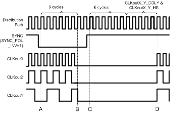
CLKout2_3_DIV = 2
CLKout4_5_DIV = 4
The digital delay for all clock outputs is 5
The digital delay half step for all clock outputs is 0
SYNC_QUAL = 0 (No qualification)
Refer to Figure 11 during this discussion on the timing of SYNC. SYNC must be asserted for greater than one clock cycle of the clock distribution path to latch the SYNC event. After SYNC is asserted, the SYNC event is latched on the rising edge of the distribution path clock, at time A. After this event has been latched, the outputs will not reflect the low state for 6 cycles, at time B. Due to the asynchronous nature of SYNC with respect to the output clocks, it is possible that a glitch pulse could be created when the clock output goes low from the SYNC event. This is shown by CLKout4 in Figure 11 and CLKout2 in Figure 12. See Relative Dynamic Digital Delay for more information on synchronizing relative to an output clock to eliminate or minimize this glitch pulse.
After SYNC becomes unasserted the event is latched on the following rising edge of the distribution path clock, time C. The clock outputs will rise at time D, coincident with a rising distribution clock edge that occurs after 6 cycles plus as many more cycles as programmed by the digital delay for that clock output. Therefore, the soonest a clock output will become high is 11 cycles after the SYNC unassertion event registration, time C, when the smallest digital delay value of 5 is set. If CLKoutX_Y_HS = 1 and CLKoutX_Y_DDLY = 5, then the clock output will rise 10.5 cycles after SYNC is unassertion event registration.
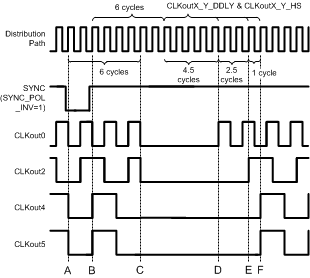
CLKout2_3_DIV = 4, CLKout2_3_DDLY = 7
CLKout4_5_DIV = 4, CLKout4_5_DDLY = 8
CLKout0_1_HS = 1
CLKout2_3_HS = 0
CLKout4_5_HS = 0
SYNC_QUAL = 0 (No qualification)
Figure 12 illustrates the timing with different digital delays programmed.
- Time A) SYNC assertion event is latched.
- Time B) SYNC unassertion latched.
- Time C) All outputs toggle and remain low. A glitch pulse can occur at this time as shown by CLKout2.
- Time D) After 6 + 4.5 = 10.5 cycles CLKout0 rises. This is the shortest time from SYNC unassertion registration to clock rising edge possible.
- Time E) After 6 + 7 = 13 cycles CLKout2 rises. CLKout2 and CLKout4, 5 are programmed for quadrature operation.
- Time F) After 6 + 8 = 14 cycles CLKout4 and 5 rise. Since CLKout4 and 5 are driven by the same clock divider and delay circuit, their timing is always the same.
8.3.9.3.5 Dynamically Programming Digital Delay
To use dynamic digital delay synchronization qualification set SYNC_QUAL = 1. This causes the SYNC pulse to be qualified by a clock output so that the SYNC event occurs after a specified time from a clock output transition. This allows the relative adjustment of clock output phase in real-time with no or minimum interruption of clock outputs. Hence the term "dynamic digital delay".
Note that changing the phase of a clock output requires momentarily altering in the rate of change of the clock output phase and therefore by definition results in a frequency distortion of the signal.
Without qualifying the SYNC with an output clock, the newly synchronized clocks would have a random and unknown digital delay (or phase) with respect to clock outputs not currently being synchronized.
8.3.9.3.5.1 Absolute vs. Relative Dynamic Digital Delay
The clock used for qualification of SYNC is selected with the feedback mux (FEEDBACK_MUX).
If the clock selected by the feedback mux has its NO_SYNC_CLKoutX_Y = 1, then an absolute dynamic digital delay adjustment will be performed during a SYNC event and the digital delay of the feedback clock will not be adjusted.
If the clock selected by the feedback mux has its NO_SYNC_CLKoutX_Y = 0, then a self-referenced or relative dynamic digital delay adjustment will be performed during a SYNC event and the digital delay of the feedback clock will be adjusted.
Clocks with NO_SYNC_CLKoutX_Y = 1 always operate without interruption.
8.3.9.3.5.2 Dynamic Digital Delay and 0-Delay Mode
When using a 0-delay mode absolute dynamic digital delay is recommended. Using relative dynamic digital delay with a 0-delay mode may result in a momentary clock loss on the adjusted clock also being used for 0-delay feedback that may result in PLL1 DLD becoming low. This may result in HOLDOVER mode being activated depending upon device configuration.
8.3.9.3.5.3 SYNC and Minimum Step Size
The minimum step size adjustment for digital delay is half a clock distribution path cycle. This is achieved by using the CLKoutX_Y_HS bit. The CLKoutX_Y_HS bit change effect is immediate without the need for SYNC. To shift digital delay using CLKoutX_Y_DDLY a SYNC signal must be generated for the change to take effect.
8.3.9.3.5.4 Programming Overview
To dynamically adjust the digital delay with respect to an existing clock output the device should be programmed as follows:
- Set SYNC_QUAL = 1 for clock output qualification.
- Set CLKout4_5_PD = 0. Required for proper operation of SYNC_QUAL = 1.
- Set EN_FEEDBACK_MUX = 1 to enable the feedback buffer.
- Set FEEDBACK_MUX to the clock output that the newly synchronized clocks will be qualified by.
- Set NO_SYNC_CLKoutX_Y = 1 for the output clocks that will continue to operate during the SYNC event. There is no interruption of output on these clocks.
- If FEEDBACK_MUX selects a clock output with NO_SYNC_CLKoutX_Y = 1, then absolute dynamic digital delay is performed.
- If FEEDBACK_MUX selects a clock output with NO_SYNC_CLKoutX_Y = 0, then self-referenced or relative dynamic digital delay is performed.
- The SYNC_EN_AUTO bit may be set to cause a SYNC event to begin when register R0 to R5 is programmed. The auto SYNC feature is a convenience since does not require the application to manually assert SYNC by toggling the SYNC_POL_INV bit or the SYNC pin when changing digital delay. However, under the following condition a special programming sequence is required if SYNC_EN_AUTO = 1:
- The CLKoutX_Y_DDLY value being set in the programmed register is 13 or more.
- Under the following condition a SYNC_EN_AUTO must = 0:
- If the application requires a digital delay resolution of half a clock distribution path cycle in relative dynamic digital delay mode because the HS bit must be fixed per Table 6 for a qualifying clock.
8.3.9.3.5.5 Internal Dynamic Digital Delay Timing
To dynamically adjust digital delay a SYNC must occur. Once the SYNC is qualified by an output clock, 3 cycles later an internal one shot pulse will occur. The width of the one shot pulse is 3 cycles. This internal one shot pulse will cause the outputs to turn off and then back on with a fixed delay with respect to the falling edge of the qualification clock. This allows for dynamic adjustments of digital delay with respect to an output clock.
The qualified SYNC timing is shown in Figure 13 for absolute dynamic digital delay and Figure 14 for relative dynamic digital delay.
8.3.9.3.5.6 Other Timing Requirements
When adjusting digital delay dynamically, the falling edge of the qualifying clock selected by the FEEDBACK_MUX must coincide with the falling edge of the clock distribution path. For this requirement to be met, program the CLKoutX_Y_HS value of the qualifying clock group according to Table 6.
Table 6. Half Step Programming Requirement of Qualifying Clock During Sync Event
| DISTRIBUTION PATH FREQUENCY | CLKoutX_Y_DIV VALUE | CLKoutX_Y_HS |
|---|---|---|
| ≥ 1.8 GHz | Even | Must = 1 during SYNC event. |
| Odd | Must = 0 during SYNC event. | |
| < 1.8 GHz | Even | Must = 0 during SYNC event. |
| Odd | Must = 1 during SYNC event. |
8.3.9.3.5.7 Absolute Dynamic Digital Delay
Absolute dynamic digital delay can be used to program a clock output to a specific phase offset from another clock output.
Pros:
- Simple direct phase adjustment with respect to another clock output.
- CLKoutX_Y_HS will remain constant for qualifying clock.
- Can easily use auto sync feature (SYNC_EN_AUTO = 1) when digital delay adjustment requires half step digital delay requirements.
- Can be used with 0-delay mode.
Cons:
- For some phase adjustments there may be a glitch pulse due to SYNC assertion.
8.3.9.3.5.7.1 Absolute Dynamic Digital Delay - Example
To illustrate the absolute dynamic digital delay adjust procedure, consider the following example.
System Requirements:
- VCO Frequency = 2949.12 MHz
- CLKout0 = 983.04 MHz (CLKout0_1_DIV = 3)
- CLKout2 = 491.52 MHz (CLKout2_3_DIV = 6)
- CLKout4 = 245.76 MHz (CLKout4_5_DIV = 12)
- For all clock outputs during initial programming:
- CLKoutX_Y_DDLY = 5
- CLKoutX_Y_HS = 1
- NO_SYNC_CLKoutX_Y = 0
The application requires the 491.52 MHz clock to be stepped in 30 degree steps (~169.5 ps), which is the minimum step resolution allowable by the clock distribution path requiring use of the half step bit (CLKoutX_Y_HS). That is 1 / 2949.52 MHz / 2 = ~169.5 ps. During the stepping of the 491.52-MHz clock, the 983.04-MHz and 245.76-MHz clock must not be interrupted.
Step 1: The device is programmed from register R0 to R30 with values that result in the device being locked and operating as desired, see the system requirements above. The phase of all the output clocks are aligned because all the digital delay and half step values were the same when the SYNC was generated by programming register R30. The timing of this is as shown in Figure 11.
Step 2: Now the registers will be programmed to prepare for changing digital delay (or phase) dynamically.
Table 7. Register Setup for Absolute Dynamic Digital Delay Example
| REGISTER | PURPOSE |
|---|---|
| SYNC_QUAL = 1 | Use a clock output for qualifying the SYNC pulse for dynamically adjusting digital delay. |
| EN_SYNC = 1 (default) | Required for SYNC functionality. |
| CLKout4_5_PD = 0 | Required when SYNC_QUAL = 1. CLKout4 and/or CLKout5 outputs may be powered down or in use. |
| EN_FEEDBACK_MUX = 1 | Enable the feedback mux for SYNC operation for dynamically adjusting digital delay. |
| FEEDBACK_MUX = 2 (CLKout4) | Use the fixed 245.76-MHz clock as the SYNC qualification clock. |
| NO_SYNC_CLKout0_1 = 1 | This clock output (983.04 MHz) won't be affected by SYNC. It will always operate without interruption. |
| NO_SYNC_CLKout4_5 = 1 | This clock output (245.76 MHz) won't be affected by SYNC. It will always operate without interruption. This clock will also be the qualifying clock in this example. |
| CLKout4_5_HS = 1 | Since CLKout4 is the qualifying clock and CLKoutX_Y_DIV is even, the half step bit must be set to 1. See Table 6. |
| SYNC_EN_AUTO = 1 | Automatic generation of SYNC is allowed for this case. |
After the registers in Table 7 have been programmed, the application may now dynamically adjust the digital delay of CLKout2 (491.52 MHz).
Step 3: Adjust digital delay of CLKout2.
Refer to Table 8 for the programming values to set a specified phase offset from the absolute reference clock. Table 8 is dependant upon the qualifying clock divide value of 12, refer to Calculating Dynamic Digital Delay Values for any Divide for information on creating tables for any divide value.
Table 8. Programming for Absolute Digital Delay Adjustment
| DEGREES OF ADJUSTMENT FROM INITIAL 491.52 MHz PHASE | PROGRAMMING | |
|---|---|---|
| +/-0 or +/-360 degrees | CLKout2_3_DDLY = 7; CLKout2_3_HS = 1 | |
| 30 degrees | -330 degrees | CLKout2_3_DDLY = 7; CLKout2_3_HS = 0 |
| 60 degrees | -300 degrees | CLKout2_3_DDLY = 8; CLKout2_3_HS = 1 |
| 90 degrees | -270 degrees | CLKout2_3_DDLY = 8; CLKout2_3_HS = 0 |
| 120 degrees | -240 degrees | CLKout2_3_DDLY = 9; CLKout2_3_HS = 1 |
| 150 degrees | -210 degrees | CLKout2_3_DDLY = 9; CLKout2_3_HS = 0 |
| 180 degrees | -180 degrees | CLKout2_3_DDLY = 10; CLKout2_3_HS = 1 |
| 210 degrees | -150 degrees | CLKout2_3_DDLY = 10; CLKout2_3_HS = 0 |
| 240 degrees | -120 degrees | CLKout2_3_DDLY = 5; CLKout2_3_HS = 1 |
| 270 degrees | -90 degrees | CLKout2_3_DDLY = 5; CLKout2_3_HS = 0 |
| 300 degrees | -60 degrees | CLKout2_3_DDLY = 6; CLKout2_3_HS = 1 |
| 330 degrees | -30 degrees | CLKout2_3_DDLY = 6; CLKout2_3_HS = 0 |
After setting the new digital delay values, the act of programming R1 will start a SYNC automatically because SYNC_EN_AUTO = 1.
If the user elects to reduce the number of SYNCs because they are not required when only CLKout2_3_HS is set, then SYNC_EN_AUTO is = 0 and the SYNC may now be generated by toggling the SYNC pin or by toggling the SYNC_POL_INV bit. Because of the internal one shot pulse, no strict timing of the SYNC pin or SYNC_POL_INV bit is required.
After the SYNC event, the clock output will adjust according to Table 8. See Figure 13 for a detailed view of the timing diagram. The timing diagram critical points are:
- Time A) SYNC assertion event is latched.
- Time B) First qualifying falling clock output edge.
- Time C) Second qualifying falling clock output edge.
- Time D) Internal one shot pulse begins. 5 cycles later clock outputs will be forced low
- Time E) Internal one shot pulse ends. 5 cycles + digital delay cycles later the synced clock outputs rise.
- Time F) Clock outputs are forced low. (CLKout2 is already low).
- Time G) Beginning of digital delay cycles.
- Time H) For CLKout2_3_DDLY = 6; the clock output rises now.
 Figure 13. Absolute Dynamic Digital Delay Programming Example
(SYNC_QUAL = 1, Qualify with Clock Output)
8.3.9.3.5.8 Relative Dynamic Digital Delay
Relative dynamic digital delay can be used to program a clock output to a specific phase offset from another clock output.
- Simple direct phase adjustment with respect to same clock output.
- The clock output will always behave the same during digital delay adjustment transient. For some divide values there will be no glitch pulse.
- For some clock divide values there may be a glitch pulse due to SYNC assertion.
- Adjustments of digital delay requiring the half step bit (CLKoutX_Y_HS) for finer digital delay adjust is complicated.
- Use with 0-delay mode may result in PLL1 DLD becoming low and HOLDOVER mode becoming activated.
- DISABLE_DLD1_DET can be set to prevent HOLDOVER from becoming activated due to PLL1 DLD becoming low.
Pros:
Cons:
8.3.9.3.5.8.1 Relative Dynamic Digital Delay - Example
To illustrate the relative dynamic digital delay adjust procedure, consider the following example.
System Requirements:
- VCO Frequency = 2949.12 MHz
- CLKout0 = 983.04 MHz (CLKout0_1_DIV = 3)
- CLKout2 = 491.52 MHz (CLKout2_3_DIV = 6)
- CLKout4 = 491.52 MHz (CLKout4_5_DIV = 6)
- For all clock outputs during initial programming:
- CLKoutX_Y_DDLY = 5
- CLKoutX_Y_HS = 0
- NO_SYNC_CLKoutX_Y = 0
The application requires the 491.52-MHz clock to be stepped in 30 degree steps (~169.5 ps), which is the minimum step resolution allowable by the clock distribution path. That is 1 / 2949.52 MHz / 2 = ~169.5 ps. During the stepping of the 491.52 MHz clocks the 983.04 MHz clock must not be interrupted.
Step 1: The device is programmed from register R0 to R30 with values that result in the device being locked and operating as desired, see the system requirements above. The phase of all the output clocks are aligned because all the digital delay and half step values were the same when the SYNC was generated by programming register R30. The timing of this is as shown in Figure 11.
Step 2: Now the registers will be programmed to prepare for changing digital delay (or phase) dynamically.
Table 9. Register Setup for Relative Dynamic Digital Delay Adjustment
| REGISTER | PURPOSE |
|---|---|
| SYNC_QUAL = 1 | Use clock output for qualifying the SYNC pulse for dynamically adjusting digital delay. |
| EN_SYNC = 1 (default) | Required for SYNC functionality. |
| CLKout4_5_PD = 0 | Required when SYNC_QUAL = 1. CLKout4 and/or CLKout5 outputs may be powered down or in use. |
| EN_FEEDBACK_MUX = 1 | Enable the feedback mux for SYNC operation for dynamically adjusting digital delay. |
| FEEDBACK_MUX = 1 (CLKout2) | Use the clock itself as the SYNC qualification clock. |
| NO_SYNC_CLKout0_1 = 1 | This clock output (983.04 MHz) won't be affected by SYNC. It will always operate without interruption. |
| NO_SYNC_CLKout4_5 = 1 | CLKout3’s phase is not to change with respect to CLKout0. |
| SYNC_EN_AUTO = 0 (default) | Automatic generation of SYNC is not allowed because of the half step requirement in relative dynamic digital delay mode. SYNC must be generated manually by toggling the SYNC_POL_INV bit or the SYNC pin. |
After the above registers have been programmed, the application may now dynamically adjust the digital delay of the 491.52 MHz clocks.
Step 3: Adjust digital delay of CLKout2 by one step which is 30 degrees or ~169.5 ps.
Refer to Table 10 for the programming sequence to step one half clock distribution period forward or backwards. Refer to Calculating Dynamic Digital Delay Values for any Divide for more information on how to calculate digital delay and half step values for other cases.
To fulfill the qualifying clock output half step requirement in Table 6 when dynamically adjusting digital delay, the CLKoutX_Y_HS bit must be cleared for clocks with even divides. So before any dynamic digital delay adjustment, CLKoutX_Y_HS must be clear because the clock divide value is even. To achieve the final required digital delay adjustment, the CLKoutX_Y_HS bit may set after SYNC.
Table 10. Programming Sequence for One Step Adjust
| STEP DIRECTION and CURRENT HS STATE | PROGRAMMING SEQUENCE |
|---|---|
| Adjust clock output one step forward. CLKout2_3_HS is 0. |
1. CLKout2_3_HS = 1. |
| Adjust clock output one step forward. CLKout2_3_HS is 1. |
1. CLKout2_3_DDLY = 9. 2. Perform SYNC event. 3. CLKout2_3_HS = 0. |
| Adjust clock output one step backward. CLKout2_3_HS is 0. |
1. CLKout2_3_HS = 1. 2. CLKout2_3_DDLY = 5. 3. Perform SYNC event. |
| Adjust clock output one step backward. CLKout2_3_HS is 1. |
1. CLKout2_3_HS = 0. |
After programing the updated CLKout2_3_DDLY and CLKout2_3_HS values, perform a SYNC event. The SYNC may be generated by toggling the SYNC pin or by toggling the SYNC_POL_INV bit. Because of the internal one shot pulse, no strict timing of the SYNC pin or SYNC_POL_INV bit is required. After the SYNC event, the clock output will be at the specified phase. See Figure 14 for a detailed view of the timing diagram. The timing diagram critical points are:
- Time A) SYNC assertion event is latched.
- Time B) First qualifying falling clock output edge.
- Time C) Second qualifying falling clock output edge.
- Time D) Internal one shot pulse begins. 5 cycles later clock outputs will be forced low.
- Time E) Internal one shot pulse ends. 5 cycles + digital delay cycles later the synced clock outputs rise.
- Time F) Clock outputs are forced low. (CLKouts are already low).
- Time G) Beginning of digital delay cycles.
- Time H) For CLKout2_3_DDLY = 9; the clock output rises now.
Starting condition is after half step is removed (CLKout2_3_HS = 0).
8.3.10 0-Delay Mode
When 0-delay mode is enabled the clock output selected by the Feedback Mux is connected to the PLL1 N counter to ensure a fixed phase relationship between the selected CLKin and the fed back CLKout. When all the clock outputs are synced together, all the clock outputs will share the same fixed phase relationship between the selected CLKin and the fed back CLKout. The feedback can be internal or external using FBCLKin port.
When 0-delay mode is enabled the lowest frequency clock output is fed back to the Feedback Mux to ensure a repeatable fixed CLKin to CLKout phase relationship between all clock outputs.
If a clock output that is not the lowest frequency output is selected for feedback, then clocks with lower frequencies will have an unknown phase relationship with respect the other clocks and clock input. There will be a number of possible phase relationships equal to Feedback_Clock_Frequency / Lower_Clock_Frequency that may occur.
The Feedback Mux selects the even clock output of any clock group for internal feedback or the FBCLKin port for external 0-delay feedback. The even clock can remain powered down as long as the CLKoutX_Y_PD bit is = 0 for its clock group.
To use 0-delay mode, the bit EN_FEEDBACK_MUX must be set (=1) to power up the feedback mux.
See PLL Programming for more information on programming PLL1_N for 0-delay mode.
When using an external VCO mode, internal 0-delay feedback must be used since the FBCLKin port is shared with the Fin input.
Table 11 outlines several registers to program for 0-delay mode.
Table 11. Programming 0-Delay Mode
8.4 Device Functional Modes
8.4.1 Mode Selection
The LMK0480x family is capable of operating in several different modes as programmed by MODE: Device Mode.
Table 12. Device Mode Selection
| MODE R11[31:27] |
PLL1 | PLL2 | PLL2 VCO | 0-DELAY | CLOCK DIST |
|---|---|---|---|---|---|
| 0 | X | X | Internal | X | |
| 2 | X | X | Internal | X | X |
| 3 | X | X | External | X | |
| 6 | X | Internal | X | ||
| 8 | X | Internal | X | X | |
| 11 | X | External | X | ||
| 15 | X | X | External | X | X |
| 16(1) | X |
In addition to selecting the device's mode of operation above, some modes require additional configuration. Also there are other features including holdover and dynamic digital delay that can also be enabled.
Table 13. Registers to Further Configure Device Mode of Operation
| REGISTER | HOLDOVER | 0-DELAY | DYNAMIC DIGITAL DELAY |
|---|---|---|---|
| HOLDOVER_MODE | 2 | — | — |
| EN_TRACK | User | — | — |
| DAC_CLK_DIV | User | — | — |
| EN_MAN_DAC | User | — | — |
| DISABLE_DLD1_DET | User | — | — |
| EN_VTUNE_RAIL_ DET |
User | — | — |
| DAC_HIGH_TRIP | User | — | — |
| DAC_LOW_TRIP | User | — | — |
| FORCE_HOLDOVER | 0 | — | — |
| SYNC_EN_AUTO | — | — | User |
| SYNC_QUAL | — | — | 1 |
| EN_SYNC | — | — | 1 |
| CLKout4_5_PD | — | — | 0 |
| EN_ FEEDBACK_MUX |
— | 1 | 1 |
| FEEDBACK_MUX | — | Feedback Clock | Qualifying Clock |
| NO_SYNC_ CLKoutX_Y |
— | — | User |
8.4.2 Operating Modes
The LMK0480x is a flexible device that can be configured for many different use cases. The following simplified block diagrams help show the user the different use cases of the device.
8.4.2.1 Dual PLL
Figure 15 illustrates the typical use case of the LMK0480x in dual loop mode. In dual loop mode the reference to PLL1 is either CLKin0 or CLKin1. An external VCXO or tunable crystal will be used to provide feedback for the first PLL and a reference to the second PLL. This first PLL cleans the jitter with the VCXO or low cost tunable crystal by using a narrow loop bandwidth. The VCXO or tunable crystal output may be buffered through the two OSCout ports and optionally on up to 4 of the CLKouts. The VCXO or tunable crystal is used as the reference to PLL2 and may be doubled using the frequency doubler. The internal VCO drives up to six divide/delay blocks which drive 12 clock outputs.
Holdover functionality is optionally available when the input reference clock is lost. Holdover works by fixing the tuning voltage of PLL1 to the VCXO or tunable crystal.
It is also possible to use an external VCO in place of PLL2's internal VCO.
 Figure 15. Simplified Functional Block Diagram for Dual Loop Mode
8.4.2.2 0-Delay Dual PLL
Figure 16 illustrates the use case of 0-delay dual loop mode. This configuration is very similar to Dual PLL except that the feedback to the first PLL is driven by a clock output. This causes the clock outputs to have deterministic phase with respect to the clock input. Since all the clock outputs can be synchronized together, all the clock outputs can be in phase with the clock input signal. The feedback to PLL1 can be connected internally as shown, or externally using FBCLKin (CLKin1) as an input port.
It is also possible to use an external VCO in place of PLL2's internal VCO.
 Figure 16. Simplified Functional Block Diagram for 0-delay Dual Loop Mode
8.4.2.3 Single PLL
Figure 17 illustrates the use case of single PLL mode. In single PLL mode only PLL2 is used and PLL1 is powered down. OSCin is used as the reference input. The internal VCO drives up to 6 divide/delay blocks which drive 12 clock outputs. The reference at OSCin can be used to drive up to 2 OSCout ports. OSCin can also optionally drive up to 4 of the clock outputs.
It is also possible to use an external VCO in place of PLL2's internal VCO.
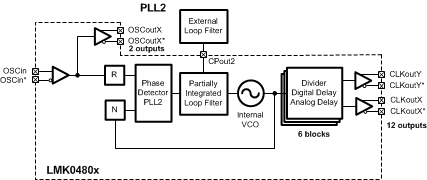 Figure 17. Simplified Functional Block Diagram for Single Loop Mode
8.4.2.4 0-Delay Single PLL
Figure 18 illustrates the use case of 0-delay single PLL mode. This configuration is very similar to Single PLL except that the feedback to PLL2 comes from a clock output. This causes the clock outputs to be in phase with the reference input. Since all the clock outputs can be synchronized together, all the clock outputs can be in phase with the clock input signal. The feedback to PLL2 can be performed internally as shown, or externally using FBCLKin (CLKin1) as an input port.
It is also possible to use an external VCO in place of PLL2's internal VCO.
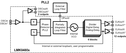 Figure 18. Simplified Functional Block Diagram for 0-delay Single Loop Mode
8.4.2.5 Clock Distribution
Figure 19 illustrates the LMK0480x used for clock distribution. CLKin1 is used to drive up to 6 divide/delay blocks which drive 12 outputs. OSCin can be used to drive up to 2 OSCout ports. OSCin can also optionally drive up to 4 of the clock outputs.
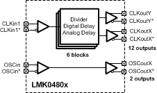 Figure 19. Simplified Functional Block Diagram for Mode Clock Distribution
8.4.2.6 Mode 15 Additional Configurations
Special considerations must be made when configuring the LMK0480x device in Dual PLL, 0-delay, External VCO mode (Mode 15). These additional registers can be programmed in sequential order as recommended or before R11 to ensure OSCoutX operation state is as desired when MODE register is programmed to 15 (0x0F).
- Program register R20 to 0x0784 E854 (This results in OSCout0 and 1 powered off. Program as desired).
- Program register R22 to 0x0000 0456
Additionally, OSCoutX power down functions are relocated to different register locations. Table 14 describes the reconfiguration of these control bits.
Table 14. Mode 15 Reconfiguration of Control Bits
| DUAL PLL, 0-DELAY, EXTERNAL VCO, MODE 15 | ALL OTHER MODES | |
|---|---|---|
| OSCout0 | PD_OSCout0 R20[23] | EN_OSCout0 R10[22] |
| 0 = OSCout0 is enabled (POR Default) | 0 = OSCout0 is disabled | |
| 1 = OSCout0 is disabled | 1 = OSCout0 is enabled (POR Default) | |
| OSCout1 | PD_OSCout1 R20[24] | EN_OSCout1 R10[23] |
| 0 = OSCout1 is enabled (POR Default) | 0 = OSCout1 is disabled (POR Default) | |
| 1 = OSCout1 is disabled | 1 = OSCout1 is enabled |
8.5 Programming
LMK0480x devices are programmed using 32-bit registers. Each register consists of a 5-bit address field and 27-bit data field. The address field is formed by bits 0 through 4 (LSBs) and the data field is formed by bits 5 through 31 (MSBs). The contents of each register is clocked in MSB first (bit 31), and the LSB (bit 0) last. During programming, the LEuWire signal should be held low. The serial data is clocked in on the rising edge of the CLKuWire signal. After the LSB (bit 0) is clocked in the LEuWire signal should be toggled low-to-high-to-low to latch the contents into the register selected in the address field. It is recommended to program registers in numeric order, for example R0 to R16, and R24 to R31 to achieve proper device operation. Figure 6 illustrates the serial data timing sequence.
To achieve proper frequency calibration, the OSCin port must be driven with a valid signal before programming register R30. Changes to PLL2 R divider or the OSCin port frequency require register R30 to be reloaded in order to activate the frequency calibration process.
8.5.1 Special Programming Case for R0 to R5 for CLKoutX_Y_DIV and CLKoutX_Y_DDLY
In some cases when programming register R0 to R5 to change the CLKoutX_Y_DIV divide value or CLKoutX_Y_DDLY delay value, 3 additional CLKuWire cycles must occur after loading the register for the newly programmed divide or delay value to take effect. These special cases include:
- When CLKoutX_Y_DIV is > 25.
- When CLKoutX_Y_DDLY is > 12. Note: loading the digital delay value only prepares for a future SYNC event.
Also, since SYNC_EN_AUTO bit = 1 automatically generates a SYNC on the falling edge of LE when R0 to R5 is programmed, further programming considerations must be made when SYNC_EN_AUTO = 1.
These special programming cases requiring the additional three clock cycles may be properly programmed by one of the following methods shown in Table 15.
Table 15. R0 to R5 Special Case
| CLKoutX_Y_DIV and CLKoutX_Y_DDLY |
SYNC _EN_ AUTO |
PROGRAMMING METHOD |
|---|---|---|
| CLKoutX_Y_DIV ≤ 25 and CLKoutX_Y_DDLY ≤ 12 |
0 or 1 | No Additional Clocks Required (Normal) |
| CLKoutX_Y_DIV > 25 or CLKoutX_Y_DDLY > 12 |
0 | Three Extra CLKuWire Clocks (Or program another register) |
| CLKoutX_Y_DIV > 25 or CLKoutX_Y_DDLY > 12 |
1 | Three Extra CLKuWire Clocks while LEuWire is High |
- Method: No Additional Clocks Required (Normal) No special consideration to CLKuWire is required when changing divide value to ≤ 25, digital delay value to ≤ 12, or when the digital delay and divide value do not change. See MICROWIRE timing Figure 6.
- Method: Three Extra CLKuWire Clocks Three extra clocks must be provided before CLKoutX_Y_DIV > 25 or CLKoutX_Y_DDLY > 12 take effect. See MICROWIRE timing Figure 7. Also, by programming another register the three clock requirement can be satisfied.
- Method: Three Extra CLKuWire Clocks with LEuWire Asserted When SYNC_EN_AUTO = 1 the falling edge of LEuWire will generate a SYNC event. CLKoutX_Y_DIV and CLKoutX_Y_DDLY values must be updated before the SYNC event occurs. So 3 CLKuWire rising edges must occur before LEuWire goes low. See MICROWIRE timing Figure 8.
- Initial Programming Sequence During the recommended programming sequence the device is programmed in order from R0 to R31, so it is expected at least one additional register will be programmed after programming the last CLKoutX_Y_DIV or CLKoutX_Y_DDLY value in R0 to R5. This will result in the extra needed CLKuWire rising edges, so this special note is of little concern. If programming R0 to R5 to change CLKout frequency or digital delay or dynamic digital delay at a later time in the application, take care to provide these extra CLKuWire cycles to properly load the new divide and/or delay values.
8.5.1.1 Example
In this example, all registers have been programmed, the PLLs are locked. An LMK04808 has been generating a clock output frequency of 61.44 MHz on CLKout4 using a VCO frequency of 2949.12 MHz and a divide value of 48. SYNC_EN_AUTO = 0. At a later time the application requires a 30.72-MHz output on CLKout4. By reprogramming register R4 with CLKout4_5_DIV = 96 twice, the divide value of 96 is set for clock outputs 4 and 5 which results in an output frequency of 30.72 MHz (2949.12 MHz / 96 = 30.72 MHz) on CLKout4.
In this example the required 3 CLKuWire cycles were achieved by reprogramming the R4 register with the same value twice.
8.5.2 Recommended Programming Sequence
Registers are programmed in numeric order with R0 being the first and R31 being the last register programmed. The recommended programming sequence involves programming R0 with the reset bit (b17) set to 1 to ensure the device is in a default state. If R0 is programmed again, the reset bit must be cleared to 0 during the programming of R0.
8.5.2.1 Overview
- Program R0 with RESET bit = 1. This ensures that the device is configured with default settings. When RESET = 1, all other R0 bits are ignored.
- If R0 is programmed again during the initial configuration of the device, the RESET bit must be cleared.
- R0 through R5: CLKouts.
- Program as necessary to configure the clock outputs, CLKout0 to CLKout11 as desired. These registers configure clock output controls such as powerdown, digital delay and divider value, analog delay select, and clock source select.
- R6 through R8: CLKouts.
- Program as necessary to configure the clock outputs, CLKout0 to CLKout11 as desired. These registers configure the output format for each clock outputs and the analog delay for the clock output groups.
- R9: Required programming
- Program this register as shown in the register map for proper operation.
- R10: OSCouts, VCO divider, and 0-delay.
- Enable and configure clock outputs OSCout0/1.
- Set and select VCO divider (VCO bypass is recommended).
- Set 0-delay feedback source if used.
- R11: Part mode, SYNC, and XTAL.
- Program to configure the mode of the part, to configure SYNC functionality and pin, and to enable crystal mode.
- R12: Pins, SYNC, and holdover mode.
- Status_LD pin, more SYNC options to generate a SYNC upon PLL1 and/or PLL2 lock detect.
- Enable clock features such as holdover.
- R13: Pins, holdover mode, and CLKins.
- Status_HOLDOVER, Status_CLKin0, and Status_CLKin1 pin controls.
- Enable clock inputs for use in specific part modes.
- R14: Pins, LOS, CLKins, and DAC.
- Status_CLKin1 pin control.
- Loss of signal detection, CLKin type, DAC rail detect enable and high and low trip points.
- R15: DAC and holdover mode.
- Program to enable and set the manual DAC value.
- HOLDOVER mode options.
- R16: Crystal amplitude.
- Increasing XTAL_LVL can improve tunable crystal phase noise performance.
- R24: PLL1 and PLL2.
- PLL1 N and R delay and PLL1 digital lock delay value.
- PLL2 integrated loop filter.
- R25: DAC and PLL1.
- Program to configure DAC update clock divider and PLL1 digital lock detect count.
- R26: PLL2.
- Program to configure PLL2 options.
- R27: CLKins and PLL1.
- Clock input pre-dividers.
- Program to configure PLL1 options.
- R28: PLL1 and PLL2.
- Program to configure PLL2 R and PLL1 N.
- R29: OSCin and PLL2.
- Program to configure oscillator input frequency, PLL2 fast phase detector frequency mode, and PLL2 N calibration value.
- R30: PLL2.
- Program to configure PLL2 prescaler and PLL2 N value.
- R31: uWire lock.
- Program to set the uWire_LOCK bit.
8.5.3 Readback
At no time should the MICROWIRE registers be programmed to any value other than what is specified in the datasheet.
For debug of the MICROWIRE interface, it is recommended to simply program an output pin mux to active low and then toggle the output type register between output and inverting output while observing the output pin for a low to high transition. For example, to verify MICROWIRE programming, set the LD_MUX = 0 (Low) and then toggle the LD_TYPE register between 3 (Output, push-pull) and 4 (Output inverted, push-pull). The result will be that the Status_LD pin will toggle from low to high.
Readback from the MICROWIRE programming registers is available. The MICROWIRE readback function can be enabled on the Status_LD, Status_HOLDOVER, Status_CLKin0, Status_CLKin1, or SYNC pin by programming the corresponding MUX register to “uWire Readback” and the corresponding TYPE register to "Output (push-pull)." Power on reset defaults the Status_HOLDOVER pin to “uWire Readback.”
Figure 9 illustrates the serial data timing sequence for a readback operation for both cases of READBACK_LE = 0 (POR default) and READBACK_LE = 1.
To perform a readback operation first set the register to be read back by programming the READBACK_ADDR register. Then after any MICROWIRE write operation, with the LEuWire pin held low continue to clock the CLKuWire pin. On every rising edge of the CLKuWire pin a new data bit is clocked onto the any pins programmed for uWire Readback. If the READBACK_LE bit is set, the LEuWire pin should be left high after LEuWire rising edge while continuing to clock the CLKuWire pin.
It is allowable to perform a register read back in the same MICROWIRE operation which set the READBACK_ADDR register value.
Data is clocked out MSB first. After 27 clocks all the data values will have been read and the read operation is complete. If READBACK_LE = 1, the LEuWire line may now be lowered. It is allowable for the CLKuWire pin to be clocked additional cycles, but the data on the readback pin will be invalid.
CLKuWire must be low before the falling edge of LEuWire.
8.5.3.1 Readback - Example
To readback register R3 perform the following steps:
- Write R31 with READBACK_ADDR = 3; READBACK_LE = 0. DATAuWire and CLKuWire are toggled as shown in Figure 6 with new data being clocked in on rising edges of CLKuWire
- Toggle LEuWire high and then low as shown in Figure 6 and Figure 9. LEuWire is returned low because READBACK_LE = 0.
- Toggle CLKuWire high and then low 27 times to read back all 27 bits of register R3. Data is read MSB first. Data is valid on falling edge of CLKuWire.
- Read operation is complete.
8.6 Register Maps
8.6.1 Register Map and Readback Register Map
Table 16 provides the register map for device programming. Normally any register can be read from the same data address it is written to. However, READBACK_LE has a different readback address. Also, the DAC_CNT register is a read only register. Table 17 shows the address for READBACK_LE and DAC_CNT. Bits marked as reserved are undefined upon readback.
Observe that only the DATA bits are readback during a readback which can result in an offset of 5 bits between the two register tables.
Table 16. Register Map
| REG- ISTER |
31 | 30 | 29 | 28 | 27 | 26 | 25 | 24 | 23 | 22 | 21 | 20 | 19 | 18 | 17 | 16 | 15 | 14 | 13 | 12 | 11 | 10 | 9 | 8 | 7 | 6 | 5 | 4 | 3 | 2 | 1 | 0 |
|---|---|---|---|---|---|---|---|---|---|---|---|---|---|---|---|---|---|---|---|---|---|---|---|---|---|---|---|---|---|---|---|---|
| Data [26:0] | Address [4:0] | |||||||||||||||||||||||||||||||
| R0 | CLKout 0_1_PD |
0 | CLKout1_ ADLY_SEL |
CLKout0_ ADLY_SEL |
CLKout0_1_DDLY [27:18] | RESET | CLKout 0_1_HS |
CLKout0_1_DIV [15:5] | 0 | 0 | 0 | 0 | 0 | |||||||||||||||||||
| R1 | CLKout 2_3_PD |
0 | CLKout3_ ADLY_SEL |
CLKout2_ ADLY_SEL |
CLKout2_3_DDLY [27:18] | POWERDOWN | CLKout 2_3_HS |
CLKout2_3_DIV [15:5] | 0 | 0 | 0 | 0 | 1 | |||||||||||||||||||
| R2 | CLKout 4_5_PD |
0 | CLKout5_ ADLY_SEL |
CLKout4_ ADLY_SEL |
CLKout4_5_DDLY [27:18] | 0 | CLKout 4_5_HS |
CLKout4_5_DIV [15:5] | 0 | 0 | 0 | 1 | 0 | |||||||||||||||||||
| R3 | CLKout 6_7_PD |
CLKout6_7_ OSCin_Sel |
CLKout7_ ADLY_SEL |
CLKout6_ ADLY_SEL |
CLKout6_7_DDLY [27:18] | 0 | CLKout 6_7_HS |
CLKout6_7_DIV [15:5] | 0 | 0 | 0 | 1 | 1 | |||||||||||||||||||
| R4 | CLKout 8_9_PD |
CLKout8_9_ OSCin_Sel |
CLKout9_ ADLY_SEL |
CLKout8_ ADLY_SEL |
CLKout8_9_DDLY [27:18] | 0 | CLKout 8_9_HS |
CLKout8_9_DIV [15:5] | 0 | 0 | 1 | 0 | 0 | |||||||||||||||||||
| R5 | CLKout 10_11_PD |
0 | CLKout11_ ADLY_SEL |
CLKout10_ ADLY_SEL |
CLKout10_11_DDLY [27:18] | 0 | CLKout 10_11_HS |
CLKout10_11_DIV [15:5] | 0 | 0 | 1 | 0 | 1 | |||||||||||||||||||
| R6 | CLKout3_TYPE [31:28] | CLKout2_TYPE [27:24] | CLKout1_TYPE [23:20] | CLKout0_TYPE [19:16] | CLKout2_3_ADLY [15:11] |
0 | CLKout0_1_ADLY [9:5] |
0 | 0 | 1 | 1 | 0 | ||||||||||||||||||||
| R7 | CLKout7_TYPE [31:28] | CLKout6_TYPE [27:24] | CLKout5_TYPE [23:20] | CLKout4_TYPE [19:16] | CLKout6_7_ADLY [15:11] |
0 | CLKout4_5_ADLY [9:5] |
0 | 0 | 1 | 1 | 1 | ||||||||||||||||||||
| R8 | CLKout11_TYPE [31:28] | CLKout10_TYPE [27:24] | CLKout9_TYPE [23:20] | CLKout8_TYPE [19:16] | CLKout10_11_ADLY [15:11] |
0 | CLKout8_9_ADLY [9:5] |
0 | 1 | 0 | 0 | 0 | ||||||||||||||||||||
| R9 | 0 | 1 | 0 | 1 | 0 | 1 | 0 | 1 | 0 | 1 | 0 | 1 | 0 | 1 | 0 | 1 | 0 | 1 | 0 | 1 | 0 | 1 | 0 | 1 | 0 | 1 | 0 | 0 | 1 | 0 | 0 | 1 |
| R10 | OSCout1_ LVPECL_ AMP [31:30] |
0 | 1 | OSCout0_TYPE [27:24] | EN_OSCout1 | EN_OSCout0 | OSCout1_MUX | OSCout0_MUX | PD_OSCin | OSCout_DIV [18:16] |
0 | 1 | 0 | VCO_MUX | EN_ FEEDBACK_MUX |
VCO_DIV [10:8] |
FEEDBACK _MUX [7:5] |
0 | 1 | 0 | 1 | 0 | ||||||||||
| R11 | MODE [31:27] | EN_SYNC | NO_SYNC_CLKout10_11 | NO_SYNC_CLKout8_9 | NO_SYNC_CLKout6_7 | NO_SYNC_CLKout4_5 | NO_SYNC_CLKout2_3 | NO_SYNC_CLKout0_1 | SYNC_MUX [19:18] |
SYNC_QUAL | SYNC_POL_INV | SYNC_EN_AUTO | SYNC_TYPE [14:12] |
0 | 0 | 0 | 0 | 0 | 0 | EN_PLL2_XTAL | 0 | 1 | 0 | 1 | 1 | |||||||
| R12 | LD_MUX [31:27] | LD_TYPE [26:24] | SYNC_PLL2 _DLD |
SYNC_PLL1 _DLD |
0 (1) |
0 | 1 | 1 | 0 | 0 | 0 | 0 | 0 | 0 | 0 | 0 | 0 | EN_TRACK | HOLDOVER _MODE [7:6] |
1 | 0 | 1 | 1 | 0 | 0 | |||||||
| R13 | HOLDOVER_MUX [31:27] |
HOLDOVER _TYPE [26:24] |
0 | Status_ CLKin1 _MUX [22:20] |
0 | Status_ CLKin0 _TYPE [18:16] |
DISABLE_ DLD1_DET |
Status_ CLKin0 _MUX [14:12] |
CLKin _Select _MODE [11:8] |
CLKin_Sel_INV | 0 | EN_CLKin1 | EN_CLKin0 | 0 | 1 | 1 | 0 | 1 | ||||||||||||||
| R14 | LOS_ TIMEOUT [31:30] |
0 | EN_LOS | 0 | Status_ CLKin1 _TYPE [26:24] |
0 | 0 | CLKin1_BUF_TYPE | CLKin0_BUF_TYPE | DAC_HIGH_TRIP [19:14] |
0 | 0 | DAC_LOW_TRIP [11:6] |
EN_VTUNE_ RAIL_DET |
0 | 1 | 1 | 1 | 0 | |||||||||||||
| R15 | MAN_DAC [31:22] |
0 | EN_MAN_DAC | HOLDOVER_DLD_CNT [19:6] |
FORCE_ HOLDOVER |
0 | 1 | 1 | 1 | 1 | ||||||||||||||||||||||
| R16 | XTAL_ LVL |
0 | 0 | 0 | 0 | 0 | 1 | 0 | 1 | 0 | 1 | 0 | 1 | 0 | 1 | 0 | 0 | 0 | 0 | 0 | 1 | 0 | 0 | 0 | 0 | 0 | 1 | 0 | 0 | 0 | 0 | |
| R24 | PLL2_C4_LF [31:28] |
PLL2_C3_LF [27:24] |
0 | PLL2_R4_LF [22:20] |
0 | PLL2_R3_LF [18:16] |
0 | PLL1_N_DLY [14:12] |
0 | PLL1_R_DLY [10:8] |
PLL1_ WND_ SIZE [7:6] |
0 | 1 | 1 | 0 | 0 | 0 | |||||||||||||||
| R25 | DAC_CLK_DIV [31:22] | 0 | 0 | PLL1_DLD_CNT [19:6] | 0 | 1 | 1 | 0 | 0 | 1 | ||||||||||||||||||||||
| R26 | PLL2_ WND_SIZE [31:30] |
EN_PLL2_ REF_2X |
PLL2_ CP_POL |
PLL2_CP _GAIN [27:26] |
1 | 1 | 1 | 0 | 1 | 0 | PLL2_DLD_CNT [19:6] |
PLL2_CP_TRI | 1 | 1 | 0 | 1 | 0 | |||||||||||||||
| R27 | 0 | 0 | 0 | PLL1_CP_POL | PLL1_CP _GAIN [27:26] |
0 | 0 | CLKin1_ PreR_DIV [23: 22] |
CLKin0_ PreR_DIV [21: 20] |
PLL1_R [19:6] |
PLL1_CP_TRI | 1 | 1 | 0 | 1 | 1 | ||||||||||||||||
| R28 | PLL2_R [31: 20] | PLL1_N [19:6] | 0 | 1 | 1 | 1 | 0 | 0 | ||||||||||||||||||||||||
| R29 | 0 | 0 | 0 | 0 | 0 | OSCin_FREQ [26:24] |
PLL2_ FAST_PDF |
PLL2_N_CAL [22:5] | 1 | 1 | 1 | 0 | 1 | |||||||||||||||||||
| R30 | 0 | 0 | 0 | 0 | 0 | PLL2_P [26:24] | 0 | PLL2_N [22:5] | 1 | 1 | 1 | 1 | 0 | |||||||||||||||||||
| R31 | 0 | 0 | 0 | 0 | 0 | 0 | 0 | 0 | 0 | 0 | READBACK _LE |
READBACK_ADDR [20:16] | 0 | 0 | 0 | 0 | 0 | 0 | 0 | 0 | 0 | 0 | uWire_LOCK | 1 | 1 | 1 | 1 | 1 | ||||
Table 17. Readback Register Map
| REG- ISTER |
RD 26 |
RD 25 |
RD 24 |
RD 23 |
RD 22 |
RD 21 |
RD 20 |
RD 19 |
RD 18 |
RD 17 |
RD 16 |
RD 15 |
RD 14 |
RD 13 |
RD 12 |
RD 11 |
RD 10 |
RD 9 |
RD 8 |
RD 7 |
RD 6 |
RD 5 |
RD 4 |
RD 3 |
RD 2 |
RD 1 |
RD 0 |
|---|---|---|---|---|---|---|---|---|---|---|---|---|---|---|---|---|---|---|---|---|---|---|---|---|---|---|---|
| Data [26:0] | |||||||||||||||||||||||||||
| RD R12 |
LD_MUX [26:22] | LD_TYPE [21:19] | SYNC_PLL2_DLD | SYNC_PLL1_DLD | READBACK_LE | 0 | 1 | 1 | 0 | 0 | 0 | 0 | 0 | 0 | 0 | 0 | 0 | EN_TRACK | HOLDOVER_ MODE [2:1] |
1 | |||||||
| RD R23 |
RESERVED [26:24] | DAC_CNT [23:14] | RESERVED [13:0] | ||||||||||||||||||||||||
| RD R31 |
RESERVED [26:10] | uWire_LOCK | |||||||||||||||||||||||||
8.6.2 Default Device Register Settings After Power On Reset
Table 18 illustrates the default register settings programmed in silicon for the LMK0480x after power on or asserting the reset bit. Capital X and Y represent numeric values.
Table 18. Default Device Register Settings after Power On/Reset
| GROUP | FIELD NAME | DEFAULT VALUE (DECIMAL) |
DEFAULT STATE | FIELD DESCRIPTION | REGISTER | BIT LOCATION (MSB:LSB) |
|---|---|---|---|---|---|---|
| Clock Output Control | CLKout0_1_PD | 1 | PD | Powerdown control for analog and digital delay, divider, and both output buffers | R0 | 31 |
| CLKout2_3_PD | 1 | PD | R1 | |||
| CLKout4_5_PD | 1 | PD | R2 | |||
| CLKout6_7_PD | 0 | Normal | R3 | |||
| CLKout8_9_PD | 0 | Normal | R4 | |||
| CLKout10_11_PD | 1 | PD | R5 | |||
| CLKout6_7_OSCin_Sel | 1 | OSCin | Selects the clock source for a clock group from internal VCO or external OSCin | R3 | 30 | |
| CLKout8_9_OSCin_Sel | 0 | VCO | R4 | 30 | ||
| CLKoutX_ADLY_SEL | 0 | None | Add analog delay for clock output | R0 to R5 | 28, 29 | |
| CLKoutX_Y_DDLY | 0 | 5 | Digital delay value | R0 to R5 | 27:18 [10] | |
| RESET | 0 | Not in reset | Performs power on reset for device | R0 | 17 | |
| POWERDOWN | 0 | Disabled (device is active) |
Device power down control | R1 | 17 | |
| CLKoutX_Y_HS | 0 | No shift | Half shift for digital delay | R0 to R5 | 16 | |
| CLKout0_1_DIV | 25 | Divide-by-25 | Divide for clock outputs | R0 | 15:5 [11] | |
| CLKout2_3_DIV | 25 | Divide-by-25 | R1 | |||
| CLKout4_5_DIV | 25 | Divide-by-25 | R2 | |||
| CLKout6_7_DIV | 1 | Divide-by-1 | R3 | |||
| CLKout8_9_DIV | 25 | Divide-by-25 | R4 | |||
| CLKout10_11_DIV | 25 | Divide-by-25 | R5 | |||
| CLKout3_TYPE | 0 | Powerdown | Individual clock output format. Select from LVDS/LVPECL/LVCMOS. | R6 | 31:28 [4] | |
| CLKout7_TYPE | 0 | Powerdown | R7 | |||
| CLKout11_TYPE | 0 | Powerdown | R8 | |||
| CLKout2_TYPE | 0 | Powerdown | R6 | 27:24 [4] | ||
| CLKout6_TYPE | 8 | LVCMOS (Norm/Norm) |
R7 | |||
| CLKout10_TYPE | 0 | Powerdown | R8 | |||
| CLKout1_TYPE | 0 | Powerdown | R6 | 23:20 [4] | ||
| CLKout5_TYPE | 0 | Powerdown | R7 | |||
| CLKout9_TYPE | 0 | Powerdown | R8 | |||
| CLKout0_TYPE | 0 | Powerdown | R6 | 19:16 [4] | ||
| CLKout4_TYPE | 0 | Powerdown | R7 | |||
| CLKout8_TYPE | 1 | LVDS | R8 | |||
| CLKoutX_Y_ADLY | 0 | No delay | Analog delay setting for clock group | R6 to R8 | 15:11, 9:5 [5] | |
| Osc Buffer Control | OSCout1_LVPECL_AMP | 2 | 1600 mVpp LVPECL | Set LVPECL amplitude | R10 | 31:30 [2] |
| OSCout0_TYPE | 1 | LVDS | OSCout0 default clock output | R10 | 27:24 [4] | |
| EN_OSCout1 | 0 | Disabled | Disable OSCout1 output buffer | R10 | 23 | |
| EN_OSCout0 | 1 | Enabled | Enable OSCout0 output buffer | R10 | 22 | |
| OSCout1_MUX | 0 | Bypass Divider | Select OSCout divider for OSCout1 or bypass | R10 | 21 | |
| OSCout0_MUX | 0 | Bypass Divider | Select OSCout divider for OSCout0 or bypass | R10 | 20 | |
| PD_OSCin | 0 | OSCin powered | Allows OSCin to be powered down. For use in clock distribution mode. | R10 | 19 | |
| OSCout_DIV | 0 | Divide-by-8 | OSCout divider value | R10 | 18:16 [3] | |
| Mode | VCO_MUX | 0 | VCO | Select VCO or VCO Divider output | R10 | 12 |
| EN_FEEDBACK_MUX | 0 | Disabled | Feedback MUX is powered down. | R10 | 11 | |
| VCO_DIV | 2 | Divide-by-2 | VCO Divide value | R10 | 10:8 [3] | |
| FEEDBACK_MUX | 0 | CLKout0 | Selects CLKout to feedback into the PLL1 N divider | R10 | 7:5 [3] | |
| MODE | 0 | Internal VCO | Device mode | R11 | 31:27 [5] | |
| Clock Synchronization | EN_SYNC | 1 | Enabled | Enables synchronization circuitry. | R11 | 26 |
| NO_SYNC_CLKout10_11 | 0 | Will sync | Disable individual clock groups from becoming synchronized. | R11 | 25 | |
| NO_SYNC_CLKout8_9 | 1 | Will not sync | R11 | 24 | ||
| NO_SYNC_CLKout6_7 | 1 | Will not sync | R11 | 23 | ||
| NO_SYNC_CLKout4_5 | 0 | Will sync | R11 | 22 | ||
| NO_SYNC_CLKout2_3 | 0 | Will sync | R11 | 21 | ||
| NO_SYNC_CLKout0_1 | 0 | Will sync | R11 | 20 | ||
| SYNC_MUX | 0 | Logic Low | Mux controlling SYNC pin when set to output | R11 | 19:18 [2] | |
| SYNC_QUAL | 0 | Not qualified | Allows SYNC operations to be qualified by a clock output. | R11 | 17 | |
| SYNC_POL_INV | 1 | Logic Low | Sets the polarity of the SYNC pin when input | R11 | 16 | |
| SYNC_EN_AUTO | 0 | Manual | SYNC is not started by programming a register R0 to R5. | R11 | 15 | |
| SYNC_TYPE | 1 | Input /w Pull-up |
SYNC IO pin type | R11 | 14:12 [3] | |
| Other Mode Control | EN_PLL2_XTAL | 0 | Disabled | Enable Crystal oscillator for OSCin | R11 | 5 |
| LD_MUX | 3 | PLL1 and 2 DLD | Lock detect mux selection when output | R12 | 31:27 [5] | |
| LD_TYPE | 3 | Output (Push-Pull) |
LD IO pin type | R12 | 26:24 [3] | |
| SYNC_PLL2_DLD | 0 | Normal | Force synchronization mode until PLL2 locks | R12 | 23 | |
| SYNC_PLL1_DLD | 0 | Normal | Force synchronization mode until PLL1 locks | R12 | 22 | |
| EN_TRACK | 1 | Enable Tracking | DAC tracking of the PLL1 tuning voltage | R12 | 8 | |
| HOLDOVER_MODE | 2 | Enable Holdover | Causes holdover to activate when lock is lost | R12 | 7:6 [2] | |
| HOLDOVER_MUX | 7 | uWire Readback | Holdover mux selection | R13 | 31:27 [5] | |
| HOLDOVER_TYPE | 3 | Output (Push-Pull) |
HOLDOVER IO pin type | R13 | 26:24 [3] | |
| Status_CLKin1_MUX | 0 | Logic Low | Status_CLKin1 pin MUX selection | R13 | 22:20 [3] | |
| Status_CLKin0_TYPE | 2 | Input /w Pull-down | Status_CLKin0 IO pin type | R13 | 18:16 [3] | |
| DISABLE_DLD1_DET | 0 | Not Disabled | Disables PLL1 DLD falling edge from causing HOLDOVER mode to be entered | R13 | 15 | |
| Status_CLKin0_MUX | 0 | Logic Low | Status_CLKin0 pin MUX selection | R13 | 14:12 [3] | |
| CLKin_SELECT_MODE | 3 | Manual Select | Mode to use in determining reference CLKin for PLL1 | R13 | 11:9 [3] | |
| CLKin_Sel_INV | 0 | Active High | Invert Status 0 and 1 pin polarity for input(2) | R13 | 8 | |
| CLKin Control | EN_CLKin1 | 1 | Usable | Set CLKin1 to be usable | R13 | 6 |
| EN_CLKin0 | 1 | Usable | Set CLKin0 to be usable | R13 | 5 | |
| LOS_TIMEOUT | 0 | 1200 ns, 420 kHz | Time until no activity on CLKin asserts LOS | R14 | 31:30 [2] | |
| EN_LOS | 1 | Enabled | Loss of Signal Detect at CLKin | R14 | 28 | |
| Status_CLKin1_TYPE | 2 | Input /w Pull-down | Status_CLKin1 pin IO pin type | R14 | 26:24 [3] | |
| CLKin1_BUF_TYPE | 0 | Bipolar | CLKin1 Buffer Type | R14 | 21 | |
| CLKin0_BUF_TYPE | 0 | Bipolar | CLKin0 Buffer Type | R14 | 20 | |
| DAC Control | DAC_HIGH_TRIP | 0 | ~50 mV from Vcc | Voltage from Vcc at which holdover mode is entered if EN_VTUNE_RAIL_DAC is enabled. | R14 | 19:14 [6] |
| DAC_LOW_TRIP | 0 | ~50 mV from GND | Voltage from GND at which holdover mode is entered if EN_VTUNE_RAIL_DAC is enabled. | R14 | 11:6 [6] | |
| EN_VTUNE_RAIL_DET | 0 | Disabled | Enable PLL1 unlock state when DAC trip points are achieved | R14 | 5 | |
| MAN_DAC | 512 | 3 V / 2 | Writing to this register will set the value for DAC when in manual override. Readback from this register is DAC value. |
R15 | 31:22 [10] | |
| EN_MAN_DAC | 0 | Disabled | Set manual DAC override | R15 | 20 | |
| HOLDOVER_DLD_CNT | 512 | 512 counts | Lock must be valid n many clocks of PLL1 PDF before holdover mode is exited. | R15 | 19:6 [14] | |
| FORCE_HOLDOVER | 0 | Holdover not forced | Forces holdover mode. | R15 | 5 | |
| XTAL_LVL | 0 | 1.65 Vpp | Sets drive power level of Crystal | R16 | 31:30 [2] | |
| PLL Control | PLL2_C4_LF | 0 | 10 pF | PLL2 integrated capacitor C4 value | R24 | 31:28 [4] |
| PLL2_C3_LF | 0 | 10 pF | PLL2 integrated capacitor C3 value | R24 | 27:24 [4] | |
| PLL2_R4_LF | 0 | 200 Ω | PLL2 integrated resistor R4 value | R24 | 22:20 [3] | |
| PLL2_R3_LF | 0 | 200 Ω | PLL2 integrated resistor R3 value | R24 | 18:16 [3] | |
| PLL1_N_DLY | 0 | No delay | Delay in PLL1 feedback path to decrease lag from input to output | R24 | 14:12 [3] | |
| PLL1_R_DLY | 0 | No delay | Delay in PLL1 reference path to increase lag from input to output | R24 | 10:8 [3] | |
| PLL1_WND_SIZE | 3 | 40 ns | Window size used for digital lock detect for PLL1 | R24 | 7:6 [2] | |
| DAC_CLK_DIV | 4 | Divide-by-4 | DAC update clock divisor. Divides PLL1 phase detector frequency. | R25 | 31:22 [10] | |
| PLL1_DLD_CNT | 1024 | 1024 cycles | Lock must be valid n many cycles before LD is asserted | R25 | 19:6 [14] | |
| PLL2_WND_SIZE | 0 | Reserved (1) |
Window size used for digital lock detect for PLL2 | R26 | 31:30 [2] | |
| EN_PLL2_REF_2X | 0 | Disabled, 1x | Doubles reference frequency of PLL2. | R26 | 29 | |
| PLL2_CP_POL | 0 | Negative | Polarity of PLL2 Charge Pump | R26 | 28 | |
| PLL2_CP_GAIN | 3 | 3.2 mA | PLL2 Charge Pump Gain | R26 | 27:26 [2] | |
| PLL2_DLD_CNT | 8192 | 8192 Counts | Number of PDF cycles which phase error must be within DLD window before LD state is asserted. | R26 | 19:6 [14] | |
| PLL2_CP_TRI | 0 | Active | PLL2 Charge Pump Active | R26 | 5 | |
| PLL1_CP_POL | 1 | Positive | Polarity of PLL1 Charge Pump | R27 | 28 | |
| PLL1_CP_GAIN | 0 | 100 uA | PLL1 Charge Pump Gain | R27 | 27:26 [2] | |
| CLKin1_PreR_DIV | 0 | Divide-by-1 | CLKin1 Pre-R divide value (1, 2, 4, or 8) | R27 | 23:22 [2] | |
| CLKin0_PreR_DIV | 0 | Divide-by-1 | CLKin0 Pre-R divide value (1, 2, 4, or 8) | R27 | 21:20 [2] | |
| PLL1_R | 96 | Divide-by-96 | PLL1 R Divider (1 to 16383) | R27 | 19:6 [14] | |
| PLL1_CP_TRI | 0 | Active | PLL1 Charge Pump Active | R27 | 5 | |
| PLL2_R | 4 | Divide-by-4 | PLL2 R Divider (1 to 4095) | R28 | 31:20 [12] | |
| PLL1_N | 192 | Divide-by-192 | PLL1 N Divider (1 to 16383) | R28 | 19:6 [14] | |
| OSCin_FREQ | 7 | 448 to 511 MHz | OSCin frequency range | R29 | 26:24 [3] | |
| PLL2_FAST_PDF | 1 | PLL2 PDF > 100 MHz | When set, PLL2 PDF of greater than 100 MHz may be used | R29 | 23 | |
| PLL2_N_CAL | 48 | Divide-by-48 | Actual PLL2 N divider value used in calibration routine. | R29 | 22:5 [18] | |
| PLL2_P | 2 | Divide-by-2 | PLL2 N Divider Prescaler (2 to 8) | R30 | 26:24 [3] | |
| PLL2_N | 48 | Divide-by-48 | PLL2 N Divider (1 to 262143) | R30 | 22:5 [18] | |
| READBACK_LE | 0 | LEuWire Low for Readback | State LEuWire pin must be in for readback | R31 | 21 | |
| READBACK_ADDR | 31 | Register 31 | Register to read back | R31 | 20:16 [5] | |
| uWire_LOCK | 0 | Writable | The values of registers R0 to R30 are lockable | R31 | 5 |
8.6.3 Register Descriptions
8.6.3.1 Register R0 TO R5
Registers R0 through R5 control the 12 clock outputs CLKout0 to CLKout11. Register R0 controls CLKout0 and CLKout1, Register R1 controls CLKout2 and CLKout3, and so on. All functions of the bits in these six registers are identical except the different registers control different clock outputs. The X and Y in CLKoutX_Y_PD, CLKoutX_ADLY_SEL, CLKoutY_ADLY_SEL, CLKoutX_Y_DDLY, CLKoutX_Y_HS, CLKoutX_Y_DIV denote the actual clock output which may be from 0 to 11 where X is even and Y is odd. Two clock outputs CLKoutX and CLKoutY form a clock output group and are often run together in bit names as CLKoutX_Y.
The RESET bit is only in register R0.
The POWERDOWN bit is only in register R1.
The CLKoutX_Y_OSCin_Sel bit is only in registers R3 and R4.
8.6.3.1.1 CLKoutX_Y_PD, Powerdown CLKoutX_Y Output Path
This bit powers down the clock group as specified by CLKoutX and CLKoutY. This includes the divider, digital delay, analog delay, and output buffers.
Table 19. CLKoutX_Y_PD
| R0-R5[31] | STATE |
|---|---|
| 0 | Power up clock group |
| 1 | Power down clock group |
8.6.3.1.2 CLKoutX_Y_OSCin_Sel, Clock Group Source
This bit sets the source for the clock output group CLKoutX_Y. The selected source will be either from a VCO via Mode Mux1 or from the OSCin buffer.
This bit is valid only for registers R3 and R4, clock groups CLKout6_7 and CLKout8_9 respectively. All other clock output groups are driven by a VCO via Mode Mux1.
Table 20. CLKoutX_Y_OSCin_Sel
| R3-R4[30] | CLOCK GROUP SOURCE |
|---|---|
| 0 | VCO |
| 1 | OSCin |
8.6.3.1.3 CLKoutY_ADLY_SEL[29], CLKoutX_ADLY_SEL[28], Select Analog Delay
These bits individually select the analog delay block (CLKoutX_Y_ADLY) for use with CLKoutX or CLKoutY. It is not required for both outputs of a clock output group to use analog delay, but if both outputs do select the analog delay block, then the analog delay will be the same for each output, CLKoutX and CLKoutY. When neither clock output uses analog delay, the analog delay block is powered down. Analog delay may not operate at frequencies above the minimum-ensured maximum output frequency of 1536 MHz.
Table 21. CLKoutY_ADLY_SEL[29], CLKoutX_ADLY_SEL[28]
| R0-R5[29] | R0-R5[28] | STATE |
|---|---|---|
| 0 | 0 | Analog delay powered down |
| 0 | 1 | Analog delay on even CLKoutX |
| 1 | 0 | Analog delay on odd CLKoutY |
| 1 | 1 | Analog delay on both CLKouts |
8.6.3.1.4 CLKoutX_Y_DDLY, Clock Channel Digital Delay
CLKoutX_Y_DDLY and CLKoutX_Y_HS sets the digital delay used for CLKoutX and CLKoutY. This value only takes effect during a SYNC event and if the NO_SYNC_CLKoutX_Y bit is cleared for this clock group. See Clock Output Synchronization (SYNC).
Programming CLKoutX_Y_DDLY can require special attention. See section Special Programming Case for R0 to R5 for CLKoutX_Y_DIV and CLKoutX_Y_DDLY for more details.
Using a CLKoutX_Y_DDLY value of 13 or greater will cause the clock group to operate in extended mode regardless of the clock group's divide value or the half step value.
One clock cycle is equal to the period of the clock distribution path. The period of the clock distribution path is equal to VCO Divider value divided by the frequency of the VCO. If the VCO divider is disabled or an external VCO is used, the VCO divide value is treated as 1.
tclock distribution path = VCO divide value / fVCO
Table 22. CLKoutX_Y_DDLY, 10 Bits
| R0-R5[27:18] | DELAY | POWER MODE |
|---|---|---|
| 0 (0x00) | 5 clock cycles | Normal Mode |
| 1 (0x01) | 5 clock cycles | |
| 2 (0x02) | 5 clock cycles | |
| 3 (0x03) | 5 clock cycles | |
| 4 (0x04) | 5 clock cycles | |
| 5 (0x05) | 5 clock cycles | |
| 6 (0x06) | 6 clock cycles | |
| 7 (0x07) | 7 clock cycles | |
| ... | ... | |
| 12 (0x0C) | 12 clock cycles | |
| 13 (0x0D) | 13 clock cycles | Extended Mode |
| ... | ... | |
| 520 (0x208) | 520 clock cycles | |
| 521 (0x209) | 521 clock cycles | |
| 522 (0x20A) | 522 clock cycles |
8.6.3.1.5 Reset
The RESET bit is located in register R0 only. Setting this bit will cause the silicon default values to be loaded. When programming register R0 with the RESET bit set, all other programmed values are ignored. After resetting the device, the register R0 must be programmed again (with RESET = 0) to set non-default values in register R0.
The reset occurs on the falling edge of the LEuWire pin which loaded R0 with RESET = 1.
The RESET bit is automatically cleared upon writing any other register. For instance, when R0 is written to again with default values.
Table 23. RESET
| R0[17] | STATE |
|---|---|
| 0 | Normal operation |
| 1 | Reset (automatically cleared) |
8.6.3.1.6 POWERDOWN
The POWERDOWN bit is located in register R1 only. Setting the bit causes the device to enter powerdown mode. Normal operation is resumed by clearing this bit via MICROWIRE.
Table 24. POWERDOWN
| R1[17] | STATE |
|---|---|
| 0 | Normal operation |
| 1 | Powerdown |
8.6.3.1.7 CLKoutX_Y_HS, Digital Delay Half Shift
This bit subtracts a half clock cycle of the clock distribution path period to the digital delay of CLKoutX and CLKoutY. CLKoutX_Y_HS is used together with CLKoutX_Y_DDLY to set the digital delay value.
When changing CLKoutX_Y_HS, the digital delay immediately takes effect without a SYNC event.
Table 25. CLKoutX_Y_HS
| R0-R5[16] | STATE |
|---|---|
| 0 | Normal |
| 1 | Subtract half of a clock distribution path period from the total digital delay |
8.6.3.1.8 CLKoutX_Y_DIV, Clock Output Divide
CLKoutX_Y_DIV sets the divide value for the clock group. The divide may be even or odd. Both even and odd divides output a 50% duty cycle clock.
Using a divide value of 26 or greater will cause the clock group to operate in extended mode regardless of the clock group's digital delay value.
Programming CLKoutX_Y_DIV can require special attention. See section Special Programming Case for R0 to R5 for CLKoutX_Y_DIV and CLKoutX_Y_DDLY for more details.
Table 26. CLKoutX_Y_DIV, 11 Bits
| R0-R5[15:5] | DIVIDE VALUE | POWER MODE |
|---|---|---|
| 0 (0x00) | Reserved | Normal Mode |
| 1 (0x01) | 1 (1) | |
| 2 (0x02) | 2 (2) | |
| 3 (0x03) | 3 | |
| 4 (0x04) | 4 (2) | |
| 5 (0x05) | 5 (2) | |
| 6 (0x06) | 6 | |
| ... | ... | |
| 24 (0x18) | 24 | |
| 25 (0x19) | 25 | |
| 26 (0x1A) | 26 | Extended Mode |
| 27 (0x1B) | 27 | |
| ... | ... | |
| 1044 (0x414) | 1044 | |
| 1045 (0x415) | 1045 |
8.6.3.2 Registers R6 TO R8
Registers R6 to R8 set the clock output types and analog delays.
8.6.3.2.1 CLKoutX_TYPE
The clock output types of the LMK0480x are individually programmable. The CLKoutX_TYPE registers set the output type of an individual clock output to LVDS, LVPECL, LVCMOS, or powers down the output buffer. Note that LVPECL supports four different amplitude levels and LVCMOS supports single LVCMOS outputs, inverted, and normal polarity of each output pin for maximum flexibility.
Table 27 shows at what register and address the specified clock output CLKoutX_TYPE register is located.
The CLKoutX_TYPE table shows the programming definition for these registers.
Table 27. CLKoutX_TYPE Programming Addresses
| CLKoutX | PROGRAMMING ADDRESS |
|---|---|
| CLKout0 | R6[19:16] |
| CLKout1 | R6[23:20] |
| CLKout2 | R6[27:24] |
| CLKout3 | R6[31:28] |
| CLKout4 | R7[19:16] |
| CLKout5 | R7[23:20] |
| CLKout6 | R7[27:24] |
| CLKout7 | R7[31:28] |
| CLKout8 | R8[19:16] |
| CLKout9 | R8[23:20] |
| CLKout10 | R8[27:24] |
| CLKout11 | R8[31:28] |
Table 28. CLKoutX_TYPE, 4 Bits
| R6-R8[31:28, 27:24, 23:20] | DEFINITION |
|---|---|
| 0 (0x00) | Power down |
| 1 (0x01) | LVDS |
| 2 (0x02) | LVPECL (700 mVpp) |
| 3 (0x03) | LVPECL (1200 mVpp) |
| 4 (0x04) | LVPECL (1600 mVpp) |
| 5 (0x05) | LVPECL (2000 mVpp) |
| 6 (0x06) | LVCMOS (Norm/Inv) |
| 7 (0x07) | LVCMOS (Inv/Norm) |
| 8 (0x08) | LVCMOS (Norm/Norm) |
| 9 (0x09) | LVCMOS (Inv/Inv)(1) |
| 10 (0x0A) | LVCMOS (Low/Norm)(1) |
| 11 (0x0A) | LVCMOS (Low/Inv)(1) |
| 12 (0x0C) | LVCMOS (Norm/Low)(1) |
| 13 (0x0D) | LVCMOS (Inv/Low)(1) |
| 14 (0x0E) | LVCMOS (Low/Low)(1) |
8.6.3.2.2 CLKoutX_Y_ADLY
These registers control the analog delay of the clock group CLKoutX_Y. Adding analog delay to the output will increase the noise floor of the output. For this analog delay to be active for a clock output, it must be selected with CLKout(X or Y)_ADL_SEL. If neither clock output in a clock group selects the analog delay, then the analog delay block is powered down. Analog delay may not operate at frequencies above the minimum-ensured maximum output frequency of 1536 MHz.
In addition to the programmed delay, a fixed 500 ps of delay will be added by engaging the delay block.
The programming addresses table shows at what register and address the specified clock output CLKoutX_Y_ADLY register is located.
The CLKoutX_Y_ADLY table shows the programming definition for these registers.
Table 29. CLKoutX_Y_ADLY Programming Addresses
| CLKoutX_Y_ADLY | PROGRAMMING ADDRESS |
|---|---|
| CLKout0_1_ADLY | R6[9:5] |
| CLKout2_3_ADLY | R6[15:11] |
| CLKout4_5_ADLY | R7[9:5] |
| CLKout6_7_ADLY | R7[15:11] |
| CLKout8_9_ADLY | R8[9:5] |
| CLKout10_11_ADLY | R8[15:11] |
Table 30. CLKoutX_Y_ADLY, 5 Bits
| R6-R8[15:11, 9:5] | DEFINITION |
|---|---|
| 0 (0x00) | 500 ps + No delay |
| 1 (0x01) | 500 ps + 25 ps |
| 2 (0x02) | 500 ps + 50 ps |
| 3 (0x03) | 500 ps + 75 ps |
| 4 (0x04) | 500 ps + 100 ps |
| 5 (0x05) | 500 ps + 125 ps |
| 6 (0x06) | 500 ps + 150 ps |
| 7 (0x07) | 500 ps + 175 ps |
| 8 (0x08) | 500 ps + 200 ps |
| 9 (0x09) | 500 ps + 225 ps |
| 10 (0x0A) | 500 ps + 250 ps |
| 11 (0x0B) | 500 ps + 275 ps |
| 12 (0x0C) | 500 ps + 300 ps |
| 13 (0x0D) | 500 ps + 325 ps |
| 14 (0x0E) | 500 ps + 350 ps |
| 15 (0x0F) | 500 ps + 375 ps |
| 16 (0x10) | 500 ps + 400 ps |
| 17 (0x11) | 500 ps + 425 ps |
| 18 (0x12) | 500 ps + 450 ps |
| 19 (0x13) | 500 ps + 475 ps |
| 20 (0x14) | 500 ps + 500 ps |
| 21 (0x15) | 500 ps + 525 ps |
| 22 (0x16) | 500 ps + 550 ps |
| 23 (0x17) | 500 ps + 575 ps |
8.6.3.3 Register R10
8.6.3.3.1 OSCout1_LVPECL_AMP, LVPECL Output Amplitude Control
The OSCout1 clock output can only be used as an LVPECL output type. OSCout1_LVPECL_AMP sets the LVPECL output amplitude of the OSCout1 clock output.
Table 31. OSCout1_LVPECL_AMP, 2 Bits
| R10[31:30] | OUTPUT FORMAT |
|---|---|
| 0 (0x00) | LVPECL (700 mVpp) |
| 1 (0x01) | LVPECL (1200 mVpp) |
| 2 (0x02) | LVPECL (1600 mVpp) |
| 3 (0x03) | LVPECL (2000 mVpp) |
8.6.3.3.2 OSCout0_TYPE
The OSCout0 clock output has a programmable output type. The OSCout0_TYPE register sets the output type to LVDS, LVPECL, LVCMOS, or powers down the output buffer. Note that LVPECL supports four different amplitude levels and LVCMOS supports dual and single LVCMOS outputs with inverted, and normal polarity of each output pin for maximum flexibility.
To turn on the output, the OSCout0_TYPE must be set to a non-power down setting and enabled with EN_OSCoutX, OSCout Output Enable.
Table 32. OSCout0_TYPE, 4 Bits
| R10[27:24] | DEFINITION |
|---|---|
| 0 (0x00) | Powerdown |
| 1 (0x01) | LVDS |
| 2 (0x02) | LVPECL (700 mVpp) |
| 3 (0x03) | LVPECL (1200 mVpp) |
| 4 (0x04) | LVPECL (1600 mVpp) |
| 5 (0x05) | LVPECL (2000 mVpp) |
| 6 (0x06) | LVCMOS (Norm/Inv) |
| 7 (0x07) | LVCMOS (Inv/Norm) |
| 8 (0x08) | LVCMOS (Norm/Norm)(1) |
| 9 (0x09) | LVCMOS (Inv/Inv)(1) |
| 10 (0x0A) | LVCMOS (Low/Norm)(1) |
| 11 (0x0B) | LVCMOS (Low/Inv)(1) |
| 12 (0x0C) | LVCMOS (Norm/Low)(1) |
| 13 (0x0D) | LVCMOS (Inv/Low)(1) |
| 14 (0x0E) | LVCMOS (Low/Low)(1) |
8.6.3.3.3 EN_OSCoutX, OSCout Output Enable
EN_OSCoutX is used to enable an oscillator buffered output.
Table 33. EN_OSCout1
| R10[23] | OUTPUT STATE |
|---|---|
| 0 | OSCout1 Disabled |
| 1 | OSCout1 Enabled |
Table 34. EN_OSCout0
| R10[22] | OUTPUT STATE |
|---|---|
| 0 | OSCout0 Disabled |
| 1 | OSCout0 Enabled |
OSCout0 note: In addition to enabling the output with EN_OSCout0. The OSCout0_TYPE must be programmed to a non-power down value for the output buffer to power up.
8.6.3.3.4 OSCoutX_MUX, Clock Output Mux
Sets OSCoutX buffer to output a divided or bypassed OSCin signal. The divisor is set by OSCout_DIV, Oscillator Output Divide.
Table 35. OSCout1_MUX
| R10[21] | MUX OUTPUT |
|---|---|
| 0 | Bypass divider |
| 1 | Divided |
Table 36. OSCout0_MUX
| R10[20] | MUX OUTPUT |
|---|---|
| 0 | Bypass divider |
| 1 | Divided |
8.6.3.3.5 PD_OSCin, OSCin Powerdown Control
Except in clock distribution mode, the OSCin buffer must always be powered up.
In clock distribution mode, the OSCin buffer must be powered down if not used.
Table 37. PD_OSCin
| R10[19] | OSCin BUFFER |
|---|---|
| 0 | Normal Operation |
| 1 | Powerdown |
8.6.3.3.6 OSCout_DIV, Oscillator Output Divide
The OSCout divider can be programmed from 2 to 8. Divide by 1 is achieved by bypassing the divider with OSCoutX_MUX, Clock Output Mux.
Note that OSCout_DIV will be in the PLL1 N feedback path if OSCout0_MUX selects divided as an output. When OSCout_DIV is in the PLL1 N feedback path, the OSCout_DIV divide value must be accounted for when programming PLL1 N.
See PLL Programming for more information on programming PLL1 to lock.
Table 38. OSCout_DIV, 3 Bits
| R10[18:16] | DIVIDE |
|---|---|
| 0 (0x00) | 8 |
| 1 (0x01) | 2 |
| 2 (0x02) | 2 |
| 3 (0x03) | 3 |
| 4 (0x04) | 4 |
| 5 (0x05) | 5 |
| 6 (0x06) | 6 |
| 7 (0x07) | 7 |
8.6.3.3.7 VCO_MUX
When the internal VCO is used, the VCO divider can be selected to divide the VCO output frequency to reduce the frequency on the clock distribution path. It is recommended to use the VCO directly unless:
- Very low output frequencies are required.
- If using the VCO divider results in three or more clock output divider/delays changing from extended to normal power mode, a small power savings may be achieved by using the VCO divider.
A consequence of using the VCO divider is a small degradation in phase noise.
8.6.3.3.8 EN_FEEDBACK_MUX
When using 0-delay or dynamic digital delay (SYNC_QUAL = 1), EN_FEEDBACK_MUX must be set to 1 to power up the feedback mux.
Table 40. EN_FEEDBACK_MUX
| R10[11] | DEFINITION |
|---|---|
| 0 | Feedback mux powered down |
| 1 | Feedback mux enabled |
8.6.3.3.9 VCO_DIV, VCO Divider
Divide value of the VCO Divider.
See PLL Programming for more information on programming PLL2 to lock.
Table 41. VCO_DIV, 3 Bits
| R10[10:8] | DIVIDE |
|---|---|
| 0 (0x00) | 8 |
| 1 (0x01) | 2 |
| 2 (0x02) | 2 |
| 3 (0x03) | 3 |
| 4 (0x04) | 4 |
| 5 (0x05) | 5 |
| 6 (0x06) | 6 |
| 7 (0x07) | 7 |
8.6.3.3.10 FEEDBACK_MUX
When in 0-delay mode, the feedback mux selects the clock output to be fed back into the PLL1 N Divider.
8.6.3.4 Register R11
8.6.3.4.1 MODE: Device Mode
MODE determines how the LMK0480x operates from a high level. Different blocks of the device can be powered up and down for specific application requirements from a dual loop architecture to clock distribution.
The LMK0480x can operate in:
- Dual PLL mode with the internal VCO or an external VCO.
- Single PLL mode uses PLL2 and powers down PLL1. OSCin is used for PLL reference input.
- Clock Distribution mode allows use of CLKin1 to distribute to clock outputs CLKout0 through CLKout11, and OSCin to distribute to OSCout0, OSCout1, and optionally CLKout6 through CLKout9.
For the PLL modes, deterministic phase delay with respect to the input can be achieved with the 0-delay mode.
For the PLL modes it is also possible to use an external VCO.
Table 43. MODE, 5 Bits
| R11[31:27] | VALUE |
|---|---|
| 0 (0x00) | Dual PLL, Internal VCO |
| 1 (0x01) | Reserved |
| 2 (0x02) | Dual PLL, Internal VCO, 0-Delay |
| 3 (0x03) | Dual PLL, External VCO (Fin) |
| 4 (0x04) | Reserved |
| 5 (0x05) | Dual PLL, External VCO (Fin), 0-Delay(1) |
| 6 (0x06) | PLL2, Internal VCO |
| 7 (0x07) | Reserved |
| 8 (0x08) | PLL2, Internal VCO, 0–Delay |
| 9 (0x09) | Reserved |
| 10 (0x0A) | Reserved |
| 11 (0x0B) | PLL2, External VCO (Fin) |
| 12 (0x0C) | Reserved |
| 13 (0x0D) | Reserved |
| 14 (0x0E) | Reserved |
| 15 (0x0F) | Dual PLL, External VCO (Fin), 0-Delay(2) |
| 16 (0x10) | Clock Distribution |
8.6.3.4.2 EN_SYNC, Enable Synchronization
The EN_SYNC bit (default on) must be enabled for synchronization to work. Synchronization is required for dynamic digital delay.
The synchronization enable may be turned off once the clocks are operating to save current. If EN_SYNC is set after it has been cleared (a transition from 0 to 1), a SYNC is generated that can disrupt the active clock outputs. Setting the NO_SYNC_CLKoutX_Y bits will prevent this SYNC pulse from affecting the output clocks. Setting the EN_SYNC bit is not a valid method for synchronizing the clock outputs. See the Clock Output Synchronization section for more information on synchronization.
Table 44. EN_SYNC
| R11[26] | DEFINITION |
|---|---|
| 0 | Synchronization disabled |
| 1 | Synchronization enabled |
8.6.3.4.3 NO_SYNC_CLKoutX_Y
The NO_SYNC_CLKoutX_Y bits prevent individual clock groups from becoming synchronized during a SYNC event. A reason to prevent individual clock groups from becoming synchronized is that during synchronization, the clock output is in a fixed low state or can have a glitch pulse.
By disabling SYNC on a clock group, it will continue to operate normally during a SYNC event.
Digital delay requires a SYNC operation to take effect. If NO_SYNC_CLKoutX_Y is set before a SYNC event, the digital delay value will be unused.
Setting the NO_SYNC_CLKoutX_Y bit has no effect on clocks already synchronized together.
Table 45. NO_SYNC_CLKoutX_Y Programming Addresses
| NO_SYNC_CLKoutX_Y | PROGRAMMING ADDRESS |
|---|---|
| CLKout0 and 1 | R11:20 |
| CLKout2 and 3 | R11:21 |
| CLKout4 and 5 | R11:22 |
| CLKout6 and 7 | R11:23 |
| CLKout8 and 9 | R11:24 |
| CLKout10 and 11 | R11:25 |
Table 46. NO_SYNC_CLKoutX_Y
| R11[25, 24, 23, 22, 21, 20] | DEFINITION |
|---|---|
| 0 | CLKoutX_Y will synchronize |
| 1 | CLKoutX_Y will not synchronize |
8.6.3.4.4 SYNC_MUX
Mux controlling SYNC pin when type is an output.
All the outputs logic is active high when SYNC_TYPE = 3 (Output). All the outputs logic is active low when SYNC_TYPE = 4 (Output Inverted). For example, when SYNC_MUX = 0 (Logic Low) and SYNC_TYPE = 3 (Output) then SYNC outputs a logic low. When SYNC_MUX = 0 (Logic Low) and SYNC_TYPE = 4 (Output Inverted) then SYNC outputs a logic high.
Table 47. SYNC_MUX, 2 Bits
| R11[19:18] | SYNC PIN OUTPUT |
|---|---|
| 0 (0x00) | Logic Low |
| 1 (0x01) | Reserved |
| 2 (0x02) | Reserved |
| 3 (0x03) | uWire Readback |
8.6.3.4.5 SYNC_QUAL
When SYNC_QUAL is set, clock outputs will be synchronized to an existing clock output selected by FEEDBACK_MUX. By using the NO_SYNC_CLKoutX_Y bits, selected clock outputs will not be interrupted during the SYNC event.
Qualifying the SYNC by an output clock means that the pulse which turns the clock outputs off and on will have a fixed time relationship to the qualifying output clock.
SYNC_QUAL = 1 requires CLKout4_5_PD = 0 for proper operation. CLKout4_TYPE and CLKout5_TYPE may be set to Powerdown mode.
See Clock Output Synchronization (SYNC) for more information.
Table 48. SYNC_QUAL
| R11[17] | MODE |
|---|---|
| 0 | No qualification |
| 1 | Qualification by clock output from feedback mux (Must set CLKout4_5_PD = 0) |
8.6.3.4.6 SYNC_POL_INV
Sets the polarity of the SYNC pin when input. When SYNC is asserted the clock outputs will transition to a low state.
See Clock Output Synchronization (SYNC) for more information on SYNC. A SYNC event can be generated by toggling this bit through the MICROWIRE interface.
Table 49. SYNC_POL_INV
| R11[16] | POLARITY |
|---|---|
| 0 | SYNC is active high |
| 1 | SYNC is active low |
8.6.3.4.7 SYNC_EN_AUTO
When set, causes a SYNC event to occur when programming register R0 to R5 to adjust digital delay values.
The SYNC event will coincide with the LEuWire pin falling edge.
Refer to Special Programming Case for R0 to R5 for CLKoutX_Y_DIV and CLKoutX_Y_DDLY for more information on possible special programming considerations when SYNC_EN_AUTO = 1.
Table 50. SYNC_EN_AUTO
| R11[15] | MODE |
|---|---|
| 0 | Manual SYNC |
| 1 | SYNC Internally Generated |
8.6.3.4.8 SYNC_TYPE
Sets the IO type of the SYNC pin.
Table 51. SYNC_TYPE, 3 Bits
| R11[14:12] | POLARITY |
|---|---|
| 0 (0x00) | Input |
| 1 (0x01) | Input /w pull-up resistor |
| 2 (0x02) | Input /w pull-down resistor |
| 3 (0x03) | Output (push-pull) |
| 4 (0x04) | Output inverted (push-pull) |
| 5 (0x05) | Output (open source) |
| 6 (0x06) | Output (open drain) |
When in output mode, the SYNC input is forced to 0 regardless of the SYNC_MUX setting. A synchronization can then be activated by uWire by programming the SYNC_POL_INV register to active low to assert SYNC. SYNC can then be released by programming SYNC_POL_INV to active high. Using this uWire programming method to create a SYNC event saves the need for an IO pin from another device.
8.6.3.4.9 EN_PLL2_XTAL
If an external crystal is being used to implement a discrete VCXO, the internal feedback amplifier must be enabled with this bit in order to complete the oscillator circuit.
Table 52. EN_PLL2_XTAL
| R11[5] | OSCILLATOR AMPLIFIER STATE |
|---|---|
| 0 | Disabled |
| 1 | Enabled |
8.6.3.5 Register R12
8.6.3.5.1 LD_MUX
LD_MUX sets the output value of the LD pin.
All the outputs logic is active high when LD_TYPE = 3 (Output). All the outputs logic is active low when LD_TYPE = 4 (Output Inverted). For example, when LD_MUX = 0 (Logic Low) and LD_TYPE = 3 (Output) then Status_LD outputs a logic low. When LD_MUX = 0 (Logic Low) and LD_TYPE = 4 (Output Inverted) then Status_LD outputs a logic high.
Table 53. LD_MUX, 5 Bits
| R12[31:27] | MODE |
|---|---|
| 0 (0x00) | Logic Low |
| 1 (0x01) | PLL1 DLD |
| 2 (0x02) | PLL2 DLD |
| 3 (0x03) | PLL1 and PLL2 DLD |
| 4 (0x04) | Holdover Status |
| 5 (0x05) | DAC Locked |
| 6 (0x06) | Reserved |
| 7 (0x07) | uWire Readback |
| 8 (0x08) | DAC Rail |
| 9 (0x09) | DAC Low |
| 10 (0x0A) | DAC High |
| 11 (0x0B) | PLL1_N |
| 12 (0x0C) | PLL1_N/2 |
| 13 (0x0D) | PLL2 N |
| 14 (0x0E) | PLL2 N/2 |
| 15 (0x0F) | PLL1_R |
| 16 (0x10) | PLL1_R/2 |
| 17 (0x11) | PLL2 R (1) |
| 18 (0x12) | PLL2 R/2 (1) |
8.6.3.5.2 LD_TYPE
Sets the IO type of the LD pin.
Table 54. LD_TYPE, 3 Bits
| R12[26:24] | POLARITY |
|---|---|
| 0 (0x00) | Reserved |
| 1 (0x01) | Reserved |
| 2 (0x02) | Reserved |
| 3 (0x03) | Output (push-pull) |
| 4 (0x04) | Output inverted (push-pull) |
| 5 (0x05) | Output (open source) |
| 6 (0x06) | Output (open drain) |
8.6.3.5.3 SYNC_PLLX_DLD
By setting SYNC_PLLX_DLD a SYNC mode will be engaged (asserted SYNC) until PLL1 and/or PLL2 locks.
SYNC_QUAL must be 0 to use this functionality.
Table 55. SYNC_PLL2_DLD
| R12[23] | SYNC MODE FORCED |
|---|---|
| 0 | No |
| 1 | Yes |
Table 56. SYNC_PLL1_DLD
| R12[22] | SYNC MODE FORCED |
|---|---|
| 0 | No |
| 1 | Yes |
8.6.3.5.4 EN_TRACK
Enable the DAC to track the PLL1 tuning voltage. For optional use in in holdover mode.
Tracking can be used to monitor PLL1 voltage by readback of DAC_CNT register in any mode.
Table 57. EN_TRACK
| R12[8] | DAC TRACKING |
|---|---|
| 0 | Disabled |
| 1 | Enabled |
8.6.3.5.5 HOLDOVER_MODE
Enable the holdover mode.
Table 58. HOLDOVER_MODE, 2 Bits
| R12[7:6] | HOLDOVER MODE |
|---|---|
| 0 | Reserved |
| 1 | Disabled |
| 2 | Enabled |
| 3 | Reserved |
8.6.3.6 Register R13
8.6.3.6.1 HOLDOVER_MUX
HOLDOVER_MUX sets the output value of the Status_Holdover pin.
The outputs are active high when HOLDOVER_TYPE = 3 (Output). The outputs are active low when HOLDOVER_TYPE = 4 (Output Inverted).
Table 59. HOLDOVER_MUX, 5 Bits
| R13[31:27] | DEFINITION |
|---|---|
| 0 (0x00) | Logic Low |
| 1 (0x01) | PLL1 DLD |
| 2 (0x02) | PLL2 DLD |
| 3 (0x03) | PLL1 and PLL2 DLD |
| 4 (0x04) | Holdover Status |
| 5 (0x05) | DAC Locked |
| 6 (0x06) | Reserved |
| 7 (0x07) | uWire Readback |
| 8 (0x08) | DAC Rail |
| 9 (0x09) | DAC Low |
| 10 (0x0A) | DAC High |
| 11 (0x0B) | PLL1 N |
| 12 (0x0C) | PLL1 N/2 |
| 13 (0x0D) | PLL2 N |
| 14 (0x0E) | PLL2 N/2 |
| 15 (0x0F) | PLL1 R |
| 16 (0x10) | PLL1 R/2 |
| 17 (0x11) | PLL2 R (1) |
| 18 (0x12) | PLL2 R/2 (1) |
8.6.3.6.2 HOLDOVER_TYPE
Sets the IO mode of the Status_Holdover pin.
Table 60. HOLDOVER_TYPE, 3 Bits
| R13[26:24] | POLARITY |
|---|---|
| 0 (0x00) | Reserved |
| 1 (0x01) | Reserved |
| 2 (0x02) | Reserved |
| 3 (0x03) | Output (push-pull) |
| 4 (0x04) | Output inverted (push-pull) |
| 5 (0x05) | Output (open source) |
| 6 (0x06) | Output (open drain) |
8.6.3.6.3 Status_CLKin1_MUX
Status_CLKin1_MUX sets the output value of the Status_CLKin1 pin. If Status_CLKin1_TYPE is set to an input type, this register has no effect. This MUX register only sets the output signal.
The outputs are active high when Status_CLKin1_TYPE = 3 (Output). The outputs are active low when Status_CLKin1_TYPE = 4 (Output Inverted).
Table 61. Status_CLKin1_MUX, 3 Bits
| R13[22:20] | DEFINITION |
|---|---|
| 0 (0x00) | Logic Low |
| 1 (0x01) | CLKin1 LOS |
| 2 (0x02) | CLKin1 Selected |
| 3 (0x03) | DAC Locked |
| 4 (0x04) | DAC Low |
| 5 (0x05) | DAC High |
| 6 (0x06) | uWire Readback |
8.6.3.6.4 Status_CLKin0_TYPE
Status_CLKin0_TYPE sets the IO type of the Status_CLKin0 pin.
Table 62. Status_CLKin0_TYPE, 3 Bits
| R13[18:16] | DEFINITION |
|---|---|
| 0 (0x00) | Input |
| 1 (0x01) | Input /w pull-up resistor |
| 2 (0x02) | Input /w pull-down resistor |
| 3 (0x03) | Output (push-pull) |
| 4 (0x04) | Output inverted (push-pull) |
| 5 (0x05) | Output (open source) |
| 6 (0x06) | Output (open drain) |
8.6.3.6.5 DISABLE_DLD1_DET
DISABLE_DLD1_DET disables the HOLDOVER mode from being activated when PLL1 lock detect signal transitions from high to low.
When using Pin Select Mode as the input clock switch mode, this bit should normally be set.
Table 63. DISABLE_DLD1_DET
| R13[15] | HOLDOVER DLD1 DETECT |
|---|---|
| 0 | PLL1 DLD causes clock switch event |
| 1 | PLL1 DLD does not cause clock switch event |
8.6.3.6.6 Status_CLKin0_MUX
CLKin0_MUX sets the output value of the Status_CLKin0 pin. If Status_CLKin0_TYPE is set to an input type, this register has no effect. This MUX register only sets the output signal.
The outputs logic is active high when Status_CLKin0_TYPE = 3 (Output). The outputs logic is active low when Status_CLKin0_TYPE = 4 (Output Inverted).
Table 64. Status_CLKin0_MUX, 3 Bits
| R13[14:12] | DIVIDE |
|---|---|
| 0 (0x00) | Logic Low |
| 1 (0x01) | CLKin0 LOS |
| 2 (0x02) | CLKin0 Selected |
| 3 (0x03) | DAC Locked |
| 4 (0x04) | DAC Low |
| 5 (0x05) | DAC High |
| 6 (0x06) | uWire Readback |
8.6.3.6.7 CLKin_SELECT_MODE
CLKin_SELECT_MODE sets the mode used in determining reference CLKin for PLL1.
Table 65. CLKin_SELECT_MODE, 3 Bits
| R13[11:9] | MODE |
|---|---|
| 0 (0x00) | CLKin0 Manual |
| 1 (0x01) | CLKin1 Manual |
| 2 (0x02) | Reserved |
| 3 (0x03) | Pin Select Mode |
| 4 (0x04) | Auto Mode |
| 5 (0x05) | Reserved |
| 6 (0x06) | Auto mode and next clock pin select |
| 7 (0x07) | Reserved |
8.6.3.7 Register 14
8.6.3.7.1 LOS_TIMEOUT
This bit controls the amount of time in which no activity on a CLKin causes LOS (Loss-of-Signal) to be asserted.
Table 69. LOS_TIMEOUT, 2 Bits
| R14[31:30] | TIMEOUT |
|---|---|
| 0 (0x00) | 1200 ns, 420 kHz |
| 1 (0x01) | 206 ns, 2.5 MHz |
| 2 (0x02) | 52.9 ns, 10 MHz |
| 3 (0x03) | 23.7 ns, 22 MHz |
8.6.3.7.2 EN_LOS
Enables the LOS (Loss-of-Signal) timeout control.
Table 70. EN_LOS
| R14[28] | LOS |
|---|---|
| 0 | Disabled |
| 1 | Enabled |
8.6.3.7.3 Status_CLKin1_TYPE
Sets the IO type of the Status_CLKin1 pin.
Table 71. Status_CLKin1_TYPE, 3 Bits
| R14[26:24] | POLARITY |
|---|---|
| 0 (0x00) | Input |
| 1 (0x01) | Input /w pull-up resistor |
| 2 (0x02) | Input /w pull-down resistor |
| 3 (0x03) | Output (push-pull) |
| 4 (0x04) | Output inverted (push-pull) |
| 5 (0x05) | Output (open source) |
| 6 (0x06) | Output (open drain) |
8.6.3.7.4 CLKinX_BUF_TYPE, PLL1 CLKinX/CLKinX* Buffer Type
There are two input buffer types for the PLL1 reference clock inputs: either bipolar or CMOS. Bipolar is recommended for differential inputs such as LVDS and LVPECL. CMOS is recommended for DC coupled single ended inputs.
When using bipolar, CLKinX and CLKinX* input pins must be AC coupled when using a differential or single ended input.
When using CMOS, CLKinX and CLKinX* input pins may be AC or DC coupled with a differential input.
When using CMOS in single ended mode, the unused clock input pin (CLKinX or CLKinX*) must be AC grounded. The used clock input pin (CLKinX* or CLKinX) may be AC or DC coupled to the signal source.
The programming addresses table shows at what register and address the specified CLKinX_BUF_TYPE bit is located.
The CLKinX_BUF_TYPE table shows the programming definition for these registers.
Table 72. CLKinX_BUF_TYPE Programming Addresses
| CLKinX_BUF_TYPE | PROGRAMMING ADDRESS |
|---|---|
| CLKin1_BUF_TYPE | R14[21] |
| CLKin0_BUF_TYPE | R14[20] |
Table 73. CLKinX_BUF_TYPE
| R14[21, 20] | CLKinX BUFFER TYPE |
|---|---|
| 0 | Bipolar |
| 1 | CMOS |
8.6.3.7.5 DAC_HIGH_TRIP
Voltage from Vcc at which holdover mode is entered if EN_VTUNE_RAIL_DAC is enabled. This will also set flags which can be monitored out Status_LD/Status_Holdover pins.
Step size is ~51 mV
Table 74. DAC_HIGH_TRIP, 6 Bits
| R14[19:14] | TRIP VOLTAGE FROM VCC (V) |
|---|---|
| 0 (0x00) | 1 × Vcc / 64 |
| 1 (0x01) | 2 × Vcc / 64 |
| 2 (0x02) | 3 × Vcc / 64 |
| 3 (0x03) | 4 × Vcc / 64 |
| 4 (0x04) | 5 × Vcc / 64 |
| ... | ... |
| 61 (0x3D) | 62 × Vcc / 64 |
| 62 (0x3E) | 63 × Vcc / 64 |
| 63 (0x3F) | 64 × Vcc / 64 |
8.6.3.7.6 DAC_LOW_TRIP
Voltage from GND at which holdover mode is entered if EN_VTUNE_RAIL_DAC is enabled. This will also set flags which can be monitored out Status_LD/Status_Holdover pins.
Step size is ~51 mV
Table 75. DAC_LOW_TRIP, 6 Bits
| R14[11:6] | TRIP VOLTAGE from GND (V) |
|---|---|
| 0 (0x00) | 1 × Vcc / 64 |
| 1 (0x01) | 2 × Vcc / 64 |
| 2 (0x02) | 3 × Vcc / 64 |
| 3 (0x03) | 4 × Vcc / 64 |
| 4 (0x04) | 5 × Vcc / 64 |
| ... | ... |
| 61 (0x3D) | 62 × Vcc / 64 |
| 62 (0x3E) | 63 × Vcc / 64 |
| 63 (0x3F) | 64 × Vcc / 64 |
8.6.3.7.7 EN_VTUNE_RAIL_DET
Enables the DAC Vtune rail detection. When the DAC achieves a specified Vtune, if this bit is enabled, the current clock input is considered invalid and an input clock switch event is generated.
Table 76. EN_VTUNE_RAIL_DET
| R14[5] | STATE |
|---|---|
| 0 | Disabled |
| 1 | Enabled |
8.6.3.8 REGISTER 15
8.6.3.8.1 MAN_DAC
Sets the DAC value when in manual DAC mode in ~3.2 mV steps.
Table 77. MAN_DAC, 10 Bits
| R15[31:22] | DAC VOLTAGE |
|---|---|
| 0 (0x00) | 0 × Vcc / 1023 |
| 1 (0x01) | 1 × Vcc / 1023 |
| 2 (0x02) | 2 × Vcc / 1023 |
| ... | ... |
| 1023 (0x3FF) | 1023 × Vcc / 1023 |
8.6.3.8.2 EN_MAN_DAC
This bit enables the manual DAC mode.
Table 78. EN_MAN_DAC
| R15[20] | DAC MODE |
|---|---|
| 0 | Automatic |
| 1 | Manual |
8.6.3.8.3 HOLDOVER_DLD_CNT
Lock must be valid for this many clocks of PLL1 PDF before holdover mode is exited.
Table 79. HOLDOVER_DLD_CNT, 14 Bits
| R15[19:6] | EXIT COUNTS |
|---|---|
| 0 (0x00) | Reserved |
| 1 (0x01) | 1 |
| 2 (0x02) | 2 |
| ... | ... |
| 16,383 (0x3FFF) | 16,383 |
8.6.3.8.4 FORCE_HOLDOVER
This bit forces the holdover mode.
When holdover is forced, if in fixed CPout1 mode (EN_TRACK = 0 or 1, EN_MAN_DAC =1) , then the DAC will set the programmed MAN_DAC value. If in tracked CPout1 mode (EN_TRACK = 1, EN_MAN_DAC = 0, EN_VTUNE_RAIL_DET = 0), then the DAC will set the current tracked DAC value.
Setting FORCE_HOLDOVER does not constitute a clock input switch event unless DISABLE_DLD1_DET = 0, since when in holdover mode, PLL1_DLD = 0 will trigger the clock input switch event.
Table 80. FORCE_HOLDOVER
| R15[5] | HOLDOVER |
|---|---|
| 0 | Disabled |
| 1 | Enabled |
8.6.3.9 Register 16
8.6.3.9.1 XTAL_LVL
Sets the peak amplitude on the tunable crystal.
Increasing this value can improve the crystal oscillator phase noise performance at the cost of increased current and higher crystal power dissipation levels.
Table 81. XTAL_LVL, 2 Bits
| R15[31:22] | PEAK AMPLITUDE(1) |
|---|---|
| 0 (0x00) | 1.65 Vpp |
| 1 (0x01) | 1.75 Vpp |
| 2 (0x02) | 1.90 Vpp |
| 3 (0x03) | 2.05 Vpp |
8.6.3.10 Register 23
This register must not be programmed, it is a readback only register.
8.6.3.11 Register 24
8.6.3.11.1 PLL2_C4_LF, PLL2 Integrated Loop Filter Component
Internal loop filter components are available for PLL2, enabling either 3rd or 4th order loop filters without requiring external components.
Internal loop filter capacitor C4 can be set according to Table 82.
Table 82. PLL2_C4_LF, 4 Bits
| R24[31:28] | LOOP FILTER CAPACITANCE (pF) |
|---|---|
| 0 (0x00) | 10 pF |
| 1 (0x01) | 15 pF |
| 2 (0x02) | 29 pF |
| 3 (0x03) | 34 pF |
| 4 (0x04) | 47 pF |
| 5 (0x05) | 52 pF |
| 6 (0x06) | 66 pF |
| 7 (0x07) | 71 pF |
| 8 (0x08) | 103 pF |
| 9 (0x09) | 108 pF |
| 10 (0x0A) | 122 pF |
| 11 (0x0B) | 126 pF |
| 12 (0x0C) | 141 pF |
| 13 (0x0D) | 146 pF |
| 14 (0x0E) | Reserved |
| 15 (0x0F) | Reserved |
8.6.3.11.2 PLL2_C3_LF, PLL2 Integrated Loop Filter Component
Internal loop filter components are available for PLL2, enabling either 3rd or 4th order loop filters without requiring external components.
Internal loop filter capacitor C3 can be set according to Table 83.
Table 83. PLL2_C3_LF, 4 Bits
| R24[27:24] | LOOP FILTER CAPACITANCE(pF) |
|---|---|
| 0 (0x00) | 10 pF |
| 1 (0x01) | 11 pF |
| 2 (0x02) | 15 pF |
| 3 (0x03) | 16 pF |
| 4 (0x04) | 19 pF |
| 5 (0x05) | 20 pF |
| 6 (0x06) | 24 pF |
| 7 (0x07) | 25 pF |
| 8 (0x08) | 29 pF |
| 9 (0x09) | 30 pF |
| 10 (0x0A) | 33 pF |
| 11 (0x0B) | 34 pF |
| 12 (0x0C) | 38 pF |
| 13 (0x0D) | 39 pF |
| 14 (0x0E) | Reserved |
| 15 (0x0F) | Reserved |
8.6.3.11.3 PLL2_R4_LF, PLL2 Integrated Loop Filter Component
Internal loop filter components are available for PLL2, enabling either 3rd or 4th order loop filters without requiring external components.
Internal loop filter resistor R4 can be set according to Table 84.
Table 84. PLL2_R4_LF, 3 Bits
| R24[22:20] | RESISTANCE |
|---|---|
| 0 (0x00) | 200 Ω |
| 1 (0x01) | 1 kΩ |
| 2 (0x02) | 2 kΩ |
| 3 (0x03) | 4 kΩ |
| 4 (0x04) | 16 kΩ |
| 5 (0x05) | Reserved |
| 6 (0x06) | Reserved |
| 7 (0x07) | Reserved |
8.6.3.11.4 PLL2_R3_LF, PLL2 Integrated Loop Filter Component
Internal loop filter components are available for PLL2, enabling either 3rd or 4th order loop filters without requiring external components.
Internal loop filter resistor R3 can be set according to Table 85.
Table 85. PLL2_R3_LF, 3 Bits
| R24[18:16] | RESISTANCE |
|---|---|
| 0 (0x00) | 200 Ω |
| 1 (0x01) | 1 kΩ |
| 2 (0x02) | 2 kΩ |
| 3 (0x03) | 4 kΩ |
| 4 (0x04) | 16 kΩ |
| 5 (0x05) | Reserved |
| 6 (0x06) | Reserved |
| 7 (0x07) | Reserved |
8.6.3.11.5 PLL1_N_DLY
Increasing delay of PLL1_N_DLY will cause the outputs to lead from CLKinX. For use in 0-delay mode.
Table 86. PLL1_N_DLY, 3 Bits
| R24[14:12] | DEFINITION |
|---|---|
| 0 (0x00) | 0 ps |
| 1 (0x01) | 205 ps |
| 2 (0x02) | 410 ps |
| 3 (0x03) | 615 ps |
| 4 (0x04) | 820 ps |
| 5 (0x05) | 1025 ps |
| 6 (0x06) | 1230 ps |
| 7 (0x07) | 1435 ps |
8.6.3.11.6 PLL1_R_DLY
Increasing delay of PLL1_R_DLY will cause the outputs to lag from CLKinX. For use in 0-delay mode.
Table 87. PLL1_R_DLY, 3 Bits
| R24[10:8] | DEFINITION |
|---|---|
| 0 (0x00) | 0 ps |
| 1 (0x01) | 205 ps |
| 2 (0x02) | 410 ps |
| 3 (0x03) | 615 ps |
| 4 (0x04) | 820 ps |
| 5 (0x05) | 1025 ps |
| 6 (0x06) | 1230 ps |
| 7 (0x07) | 1435 ps |
8.6.3.11.7 PLL1_WND_SIZE
PLL1_WND_SIZE sets the window size used for digital lock detect for PLL1. If the phase error between the reference and feedback of PLL1 is less than specified time, then the PLL1 lock counter increments.
Refer to Digital Lock Detect Frequency Accuracy for more information.
Table 88. PLL1_WND_SIZE, 2 Bits
| R24[7:6] | DEFINITION |
|---|---|
| 0 | 5.5 ns |
| 1 | 10 ns |
| 2 | 18.6 ns |
| 3 | 40 ns |
8.6.3.12 Register 25
8.6.3.12.1 DAC_CLK_DIV
The DAC update clock frequency is the PLL1 phase detector frequency divided by the divisor listed in Table 89.
Table 89. DAC_CLK_DIV, 10 Bits
| R25[31:22] | DIVIDE |
|---|---|
| 0 (0x00) | Reserved |
| 1 (0x01) | 1 |
| 2 (0x02) | 2 |
| 3 (0x03) | 3 |
| ... | ... |
| 1,022 (0x3FE) | 1022 |
| 1,023 (0x3FF) | 1023 |
8.6.3.12.2 PLL1_DLD_CNT
The reference and feedback of PLL1 must be within the window of phase error as specified by PLL1_WND_SIZE for this many phase detector cycles before PLL1 digital lock detect is asserted.
Refer to Digital Lock Detect Frequency Accuracy for more information.
8.6.3.13 Register 26
8.6.3.13.1 PLL2_WND_SIZE
PLL2_WND_SIZE sets the window size used for digital lock detect for PLL2. If the phase error between the reference and feedback of PLL2 is less than specified time, then the PLL2 lock counter increments. This value must be programmed to 2 (3.7 ns).
Refer to Digital Lock Detect Frequency Accuracy for more information.
8.6.3.13.2 EN_PLL2_REF_2X, PLL2 Reference Frequency Doubler
Enabling the PLL2 reference frequency doubler allows for higher phase detector frequencies on PLL2 than would normally be allowed with the given VCXO or Crystal frequency.
Higher phase detector frequencies reduces the PLL N values which makes the design of wider loop bandwidth filters possible.
Table 92. EN_PLL2_REF_2X
| R26[29] | DESCRIPTION |
|---|---|
| 0 | Reference frequency normal |
| 1 | Reference frequency doubled (2x). See PLL2 Frequency Doubler |
8.6.3.13.3 PLL2_CP_POL, PLL2 Charge Pump Polarity
PLL2_CP_POL sets the charge pump polarity for PLL2. The internal VCO requires the negative charge pump polarity to be selected. Many VCOs use positive slope.
A positive slope VCO increases output frequency with increasing voltage. A negative slope VCO decreases output frequency with increasing voltage.
Table 93. PLL2_CP_POL
| R26[28] | DESCRIPTION |
|---|---|
| 0 | Negative Slope VCO/VCXO |
| 1 | Positive Slope VCO/VCXO |
8.6.3.13.4 PLL2_CP_GAIN, PLL2 Charge Pump Current
This bit programs the PLL2 charge pump output current level. Table 94 also illustrates the impact of the PLL2 TRI-STATE bit in conjunction with PLL2_CP_GAIN.
Table 94. PLL2_CP_GAIN, 2 Bits
| R26[27:26] | PLL2_CP_TRI R26[5] |
CHARGE PUMP CURRENT (µA) |
|---|---|---|
| X | 1 | Hi-Z |
| 0 (0x00) | 0 | 100 |
| 1 (0x01) | 0 | 400 |
| 2 (0x02) | 0 | 1600 |
| 3 (0x03) | 0 | 3200 |
8.6.3.13.5 PLL2_DLD_CNT
The reference and feedback of PLL2 must be within the window of phase error as specified by PLL2_WND_SIZE for PLL2_DLD_CNT cycles before PLL2 digital lock detect is asserted.
Refer to Digital Lock Detect Frequency Accuracy for more information
8.6.3.13.6 PLL2_CP_TRI, PLL2 Charge Pump TRI-STATE
This bit allows for the PLL2 charge pump output pin, CPout2, to be placed into TRI-STATE.
Table 96. PLL2_CP_TRI
| R26[5] | DESCRIPTION |
|---|---|
| 0 | PLL2 CPout2 is active |
| 1 | PLL2 CPout2 is at TRI-STATE |
8.6.3.14 REGISTER 27
8.6.3.14.1 PLL1_CP_POL, PLL1 Charge Pump Polarity
PLL1_CP_POL sets the charge pump polarity for PLL1. Many VCXOs use positive slope.
A positive slope VCXO increases output frequency with increasing voltage. A negative slope VCXO decreases output frequency with increasing voltage.
Table 97. PLL1_CP_POL
| R27[28] | DESCRIPTION |
|---|---|
| 0 | Negative Slope VCO/VCXO |
| 1 | Positive Slope VCO/VCXO |
8.6.3.14.2 PLL1_CP_GAIN, PLL1 Charge Pump Current
This bit programs the PLL1 charge pump output current level. Table 98 also illustrates the impact of the PLL1 TRI-STATE bit in conjunction with PLL1_CP_GAIN.
Table 98. PLL1_CP_GAIN, 2 Bits
| R26[27:26] | PLL1_CP_TRI R27[5] |
CHARGE PUMP CURRENT (µA) |
|---|---|---|
| X | 1 | Hi-Z |
| 0 (0x00) | 0 | 100 |
| 1 (0x01) | 0 | 200 |
| 2 (0x02) | 0 | 400 |
| 3 (0x03) | 0 | 1600 |
8.6.3.14.3 CLKinX_PreR_DIV
The pre-R dividers before the PLL1 R divider can be programmed such that when the active clock input is switched, the frequency at the input of the PLL1 R divider will be the same. This allows PLL1 to stay in lock without needing to re-program the PLL1 R register when different clock input frequencies are used. This is especially useful in the auto CLKin switching modes.
Table 99. CLKinX_PreR_DIV Programming Addresses
| CLKinX_PreR_DIV | PROGRAMMING ADDRESS |
|---|---|
| CLKin1_PreR_DIV | R27[23:22] |
| CLKin0_PreR_DIV | R27[21:20] |
Table 100. CLKinX_PreR_DIV, 2 Bits
| R27[23:22, 21:20] | DIVIDE |
|---|---|
| 0 (0x00) | 1 |
| 1 (0x01) | 2 |
| 2 (0x02) | 4 |
| 3 (0x03) | 8 |
8.6.3.14.4 PLL1_R, PLL1 R Divider
The reference path into the PLL1 phase detector includes the PLL1 R divider. Refer to PLL Programming for more information on how to program the PLL dividers to lock the PLL.
The valid values for PLL1_R are shown in Table 101.
Table 101. PLL1_R, 14 Bits
| R27[19:6] | DIVIDE |
|---|---|
| 0 (0x00) | Reserved |
| 1 (0x01) | 1 |
| 2 (0x02) | 2 |
| 3 (0x03) | 3 |
| ... | ... |
| 16,382 (0x3FFE) | 16,382 |
| 16,383 (0x3FFF) | 16,383 |
8.6.3.14.5 PLL1_CP_TRI, PLL1 Charge Pump TRI-STATE
This bit allows for the PLL1 charge pump output pin, CPout1, to be placed into TRI-STATE.
Table 102. PLL1_CP_TRI
| R27[5] | DESCRIPTION |
|---|---|
| 0 | PLL1 CPout1 is active |
| 1 | PLL1 CPout1 is at TRI-STATE |
8.6.3.15 Register 28
8.6.3.15.1 PLL2_R, PLL2 R Divider
The reference path into the PLL2 phase detector includes the PLL2 R divider.
Refer to PLL Programming for more information on how to program the PLL dividers to lock the PLL.
The valid values for PLL2_R are shown in Table 103.
Table 103. PLL2_R, 12 Bits
| R28[31:20] | DIVIDE |
|---|---|
| 0 (0x00) | Not Valid |
| 1 (0x01) | 1(1).
See PLL2 Frequency Doubler |
| 2 (0x02) | 2 |
| 3 (0x03) | 3 |
| ... | ... |
| 4,094 (0xFFE) | 4,094 |
| 4,095 (0xFFF) | 4,095 |
8.6.3.15.2 PLL1_N, PLL1 N Divider
The feedback path into the PLL1 phase detector includes the PLL1 N divider.
Refer to PLL Programming for more information on how to program the PLL dividers to lock the PLL.
The valid values for PLL1_N are shown in Table 104.
Table 104. PLL1_N, 14 Bits
| R28[19:6] | DIVIDE |
|---|---|
| 0 (0x00) | Not Valid |
| 1 (0x01) | 1 |
| 2 (0x02) | 2 |
| ... | ... |
| 4,095 (0xFFF) | 4,095 |
8.6.3.16 Register 29
8.6.3.16.1 OSCin_FREQ, PLL2 Oscillator Input Frequency Register
The frequency of the PLL2 reference input to the PLL2 Phase Detector (OSCin/OSCin* port) must be programmed in order to support proper operation of the frequency calibration routine which locks the internal VCO to the target frequency.
Table 105. OSCin_FREQ, 3 Bits
| R29[26:24] | OSCin FREQUENCY |
|---|---|
| 0 (0x00) | 0 to 63 MHz |
| 1 (0x01) | >63 MHz to 127 MHz |
| 2 (0x02) | >127 MHz to 255 MHz |
| 3 (0x03) | Reserved |
| 4 (0x04) | >255 MHz to 400 MHz |
8.6.3.16.2 PLL2_FAST_PDF, High PLL2 Phase Detector Frequency
When PLL2 phase detector frequency is greater than 100 MHz, set the PLL2_FAST_PDF to ensure proper operation of device.
Table 106. PLL2_FAST_PDF
| R29[23] | PLL2 PDF |
|---|---|
| 0 | Less than or equal to 100 MHz |
| 1 | Greater than 100 MHz |
8.6.3.16.3 PLL2_N_CAL, PLL2 N Calibration Divider
During the frequency calibration routine, the PLL uses the divide value of the PLL2_N_CAL register instead of the divide value of the PLL2_N register to lock the VCO to the target frequency.
NOTE: Unless in 0-delay mode, PLL2_N_CAL should be set equal to PLL2_N
Refer to PLL Programming for more information on how to program the PLL dividers to lock the PLL.
Table 107. PLL2_N_CAL, 18 Bits
| R29[22:5] | DIVIDE |
|---|---|
| 0 (0x00) | Not Valid |
| 1 (0x01) | 1 |
| 2 (0x02) | 2 |
| ... | ... |
| 262,143 (0x3FFFF) | 262,143 |
8.6.3.17 Register 30
If an internal VCO mode is used, programming Register 30 triggers the frequency calibration routine. This calibration routine will also generate a SYNC event. See Clock Output Synchronization (SYNC) for more details on a SYNC.
8.6.3.17.1 PLL2_P, PLL2 N Prescaler Divider
The PLL2 N Prescaler divides the output of the VCO as selected by VCO_MUX and is connected to the PLL2 N divider.
Refer to PLL Programming for more information on how to program the PLL dividers to lock the PLL.
Table 108. PLL2_P, 3 Bits
| R30[26:24] | DIVIDE VALUE |
| 0 (0x00) | 8 |
| 1 (0x01) | 2 |
| 2 (0x02) | 2 |
| 3 (0x03) | 3 |
| 4 (0x04) | 4 |
| 5 (0x05) | 5 |
| 6 (0x06) | 6 |
| 7 (0x07) | 7 |
8.6.3.17.2 PLL2_N, PLL2 N Divider
The feeback path into the PLL2 phase detector includes the PLL2 N divider.
Each time register 30 is updated via the MICROWIRE interface, a frequency calibration routine runs to lock the VCO to the target frequency. During this calibration PLL2_N is substituted with PLL2_N_CAL.
Refer to PLL Programming for more information on how to program the PLL dividers to lock the PLL.
The valid values for PLL2_N are shown in Table 109.
Table 109. PLL2_N, 18 Bits
| R30[22:5] | DIVIDE |
|---|---|
| 0 (0x00) | Not Valid |
| 1 (0x01) | 1 |
| 2 (0x02) | 2 |
| ... | |
| 262,143 (0x3FFFF) | 262,143 |
8.6.3.18 Register 31
8.6.3.18.1 READBACK_LE
Sets the required state of the LEuWire pin when performing register readback.
Refer to Readback.
8.6.3.18.2 READBACK_ADDR
Sets the address of the register to read back when performing readback.
When reading register 12, the READBACK_ADDR will be read back at R12[20:16].
When reading back from R31 bits 6 to 31 should be ignored. Only uWire_LOCK is valid.
Refer to Register Readback for more information on readback.
Table 111. READBACK_ADDR, 5 Bits
| R31[20:16] | REGISTER |
|---|---|
| 0 (0x00) | R0 |
| 1 (0x01) | R1 |
| 2 (0x02) | R2 |
| 3 (0x03) | R3 |
| 4 (0x04) | R4 |
| 5 (0x05) | R5 |
| 6 (0x06) | R6 |
| 7 (0x07) | R7 |
| 8 (0x08) | R8 |
| 9 (0x09) | Reserved |
| 10 (0x0A) | R10 |
| 11 (0x0B) | R11 |
| 12 (0x0C) | R12 |
| 13 (0x0D) | R13 |
| 14 (0x0E) | R14 |
| 15 (0x0F) | R15 |
| 16 (0x10) | Reserved |
| 17 (0x11) | Reserved |
| ... | ... |
| 22 (0x16) | Reserved |
| 23 (0x17) | Reserved |
| 24 (0x18) | R24 |
| 25 (0x19) | R25 |
| 26 (0x1A) | R26 |
| 27 (0x1B) | R27 |
| 28 (0x1C) | R28 |
| 29 (0x1D) | R29 |
| 30 (0x1E) | R30 |
| 31 (0x1F) | R31 |
8.6.3.18.3 uWire_LOCK
Setting uWire_LOCK will prevent any changes to uWire registers R0 to R30. Only by clearing the uWire_LOCK bit in R31 can the uWire registers be unlocked and written to once more.
It is not necessary to lock the registers to perform a readback operation.
Table 112. uWire_LOCK
| R31[5] | STATE |
|---|---|
| 0 | Registers unlocked |
| 1 | Registers locked, Write-protect |