SNAS489K March 2011 – December 2014 LMK04803 , LMK04805 , LMK04806 , LMK04808
PRODUCTION DATA.
- 1 Features
- 2 Applications
- 3 Description
- 4 Revision History
- 5 Pin Configuration and Functions
- 6 Specifications
-
7 Parameter Measurement Information
- 7.1
Charge Pump Current Specification Definitions
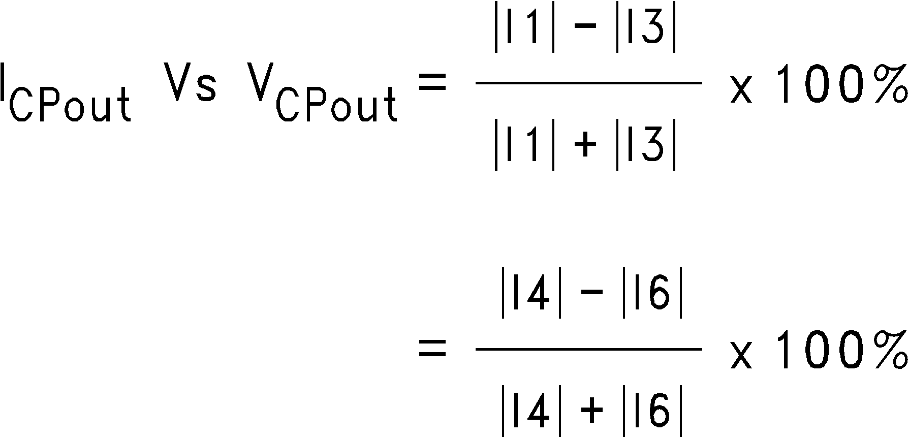
- 7.1.1 Charge Pump Output Current Magnitude Variation Vs. Charge Pump Output Voltage
- 7.1.2 Charge Pump Sink Current Vs. Charge Pump Output Source Current Mismatch
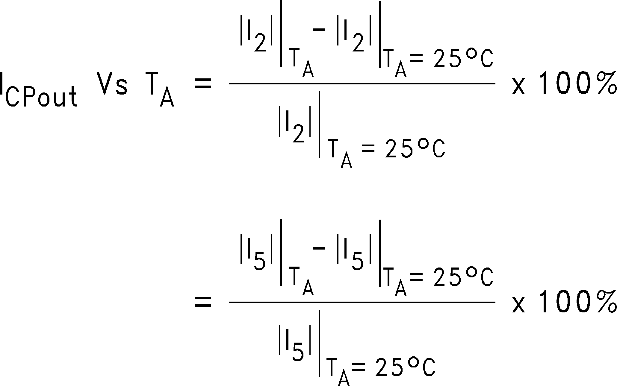
- 7.1.3 Charge Pump Output Current Magnitude Variation vs. Ambient Temperature"Temperature" to "Ambient Temperature" in heading titled "Charge Pump Output Current Magnitude Variation vs. Ambient Temperature"
- 7.2 Differential Voltage Measurement Terminology
- 7.1
Charge Pump Current Specification Definitions
-
8 Detailed Description
- 8.1
Overview
- 8.1.1 System Architecture
- 8.1.2 PLL1 Redundant Reference Inputs (CLKin0/CLKin0* and CLKin1/CLKin1*)
- 8.1.3 PLL1 Tunable Crystal Support
- 8.1.4 VCXO/CRYSTAL Buffered Outputs
- 8.1.5 Frequency Holdover
- 8.1.6 Integrated Loop Filter Poles
- 8.1.7 Internal VCO
- 8.1.8 External VCO Mode
- 8.1.9 Clock Distribution
- 8.1.10 0-Delay
- 8.1.11 Default Startup Clocks
- 8.1.12 Status Pins
- 8.1.13 Register Readback
- 8.2 Functional Block Diagram
- 8.3
Feature Description
- 8.3.1 Serial MICROWIRE Timing Diagram
- 8.3.2 Advanced MICROWIRE Timing Diagrams
- 8.3.3 Inputs / Outputs
- 8.3.4 Input Clock Switching
- 8.3.5 Holdover Mode
- 8.3.6 PLLs
- 8.3.7 Status Pins
- 8.3.8 VCO
- 8.3.9
Clock Distribution
- 8.3.9.1 Fixed Digital Delay
- 8.3.9.2 Fixed Digital Delay - Example
- 8.3.9.3
Clock Output Synchronization (SYNC)
- 8.3.9.3.1 Effect of SYNC
- 8.3.9.3.2 Methods of Generating SYNC
- 8.3.9.3.3 Avoiding Clock Output Interruption Due to Sync
- 8.3.9.3.4 SYNC Timing
- 8.3.9.3.5
Dynamically Programming Digital Delay
- 8.3.9.3.5.1 Absolute vs. Relative Dynamic Digital Delay
- 8.3.9.3.5.2 Dynamic Digital Delay and 0-Delay Mode
- 8.3.9.3.5.3 SYNC and Minimum Step Size
- 8.3.9.3.5.4 Programming Overview
- 8.3.9.3.5.5 Internal Dynamic Digital Delay Timing
- 8.3.9.3.5.6 Other Timing Requirements
- 8.3.9.3.5.7 Absolute Dynamic Digital Delay
- 8.3.9.3.5.8 Relative Dynamic Digital Delay
- 8.3.10 0-Delay Mode
- 8.4 Device Functional Modes
- 8.5 Programming
- 8.6
Register Maps
- 8.6.1 Register Map and Readback Register Map
- 8.6.2 Default Device Register Settings After Power On Reset
- 8.6.3
Register Descriptions
- 8.6.3.1
Register R0 TO R5
- 8.6.3.1.1 CLKoutX_Y_PD, Powerdown CLKoutX_Y Output Path
- 8.6.3.1.2 CLKoutX_Y_OSCin_Sel, Clock Group Source
- 8.6.3.1.3 CLKoutY_ADLY_SEL[29], CLKoutX_ADLY_SEL[28], Select Analog Delay
- 8.6.3.1.4 CLKoutX_Y_DDLY, Clock Channel Digital Delay
- 8.6.3.1.5 Reset
- 8.6.3.1.6 POWERDOWN
- 8.6.3.1.7 CLKoutX_Y_HS, Digital Delay Half Shift
- 8.6.3.1.8 CLKoutX_Y_DIV, Clock Output Divide
- 8.6.3.2 Registers R6 TO R8
- 8.6.3.3
Register R10
- 8.6.3.3.1 OSCout1_LVPECL_AMP, LVPECL Output Amplitude Control
- 8.6.3.3.2 OSCout0_TYPE
- 8.6.3.3.3 EN_OSCoutX, OSCout Output Enable
- 8.6.3.3.4 OSCoutX_MUX, Clock Output Mux
- 8.6.3.3.5 PD_OSCin, OSCin Powerdown Control
- 8.6.3.3.6 OSCout_DIV, Oscillator Output Divide
- 8.6.3.3.7 VCO_MUX
- 8.6.3.3.8 EN_FEEDBACK_MUX
- 8.6.3.3.9 VCO_DIV, VCO Divider
- 8.6.3.3.10 FEEDBACK_MUX
- 8.6.3.4 Register R11
- 8.6.3.5 Register R12
- 8.6.3.6 Register R13
- 8.6.3.7 Register 14
- 8.6.3.8 REGISTER 15
- 8.6.3.9 Register 16
- 8.6.3.10 Register 23
- 8.6.3.11
Register 24
- 8.6.3.11.1 PLL2_C4_LF, PLL2 Integrated Loop Filter Component
- 8.6.3.11.2 PLL2_C3_LF, PLL2 Integrated Loop Filter Component
- 8.6.3.11.3 PLL2_R4_LF, PLL2 Integrated Loop Filter Component
- 8.6.3.11.4 PLL2_R3_LF, PLL2 Integrated Loop Filter Component
- 8.6.3.11.5 PLL1_N_DLY
- 8.6.3.11.6 PLL1_R_DLY
- 8.6.3.11.7 PLL1_WND_SIZE
- 8.6.3.12 Register 25
- 8.6.3.13 Register 26
- 8.6.3.14 REGISTER 27
- 8.6.3.15 Register 28
- 8.6.3.16 Register 29
- 8.6.3.17 Register 30
- 8.6.3.18 Register 31
- 8.6.3.1
Register R0 TO R5
- 8.1
Overview
-
9 Application and Implementation
- 9.1
Application Information
- 9.1.1 Loop Filter
- 9.1.2 Driving CLKin and OSCin Inputs
- 9.1.3 Termination and Use of Clock Output (Drivers)
- 9.1.4 Frequency Planning with the LMK0480x Family
- 9.1.5 PLL Programming
- 9.1.6 Digital Lock Detect Frequency Accuracy
- 9.1.7 Calculating Dynamic Digital Delay Values for any Divide
- 9.1.8 Optional Crystal Oscillator Implementation (OSCin/OSCin*)
- 9.1.9 Application Curves
- 9.2 Typical Applications
- 9.3 System Examples
- 9.4 Do's and Don'ts
- 9.1
Application Information
- 10Power Supply Recommendations
- 11Layout
- 12Device and Documentation Support
- 13Mechanical, Packaging, and Orderable Information
Package Options
Mechanical Data (Package|Pins)
- NKD|64
Thermal pad, mechanical data (Package|Pins)
- NKD|64
Orderable Information
7 Parameter Measurement Information
7.1 Charge Pump Current Specification Definitions
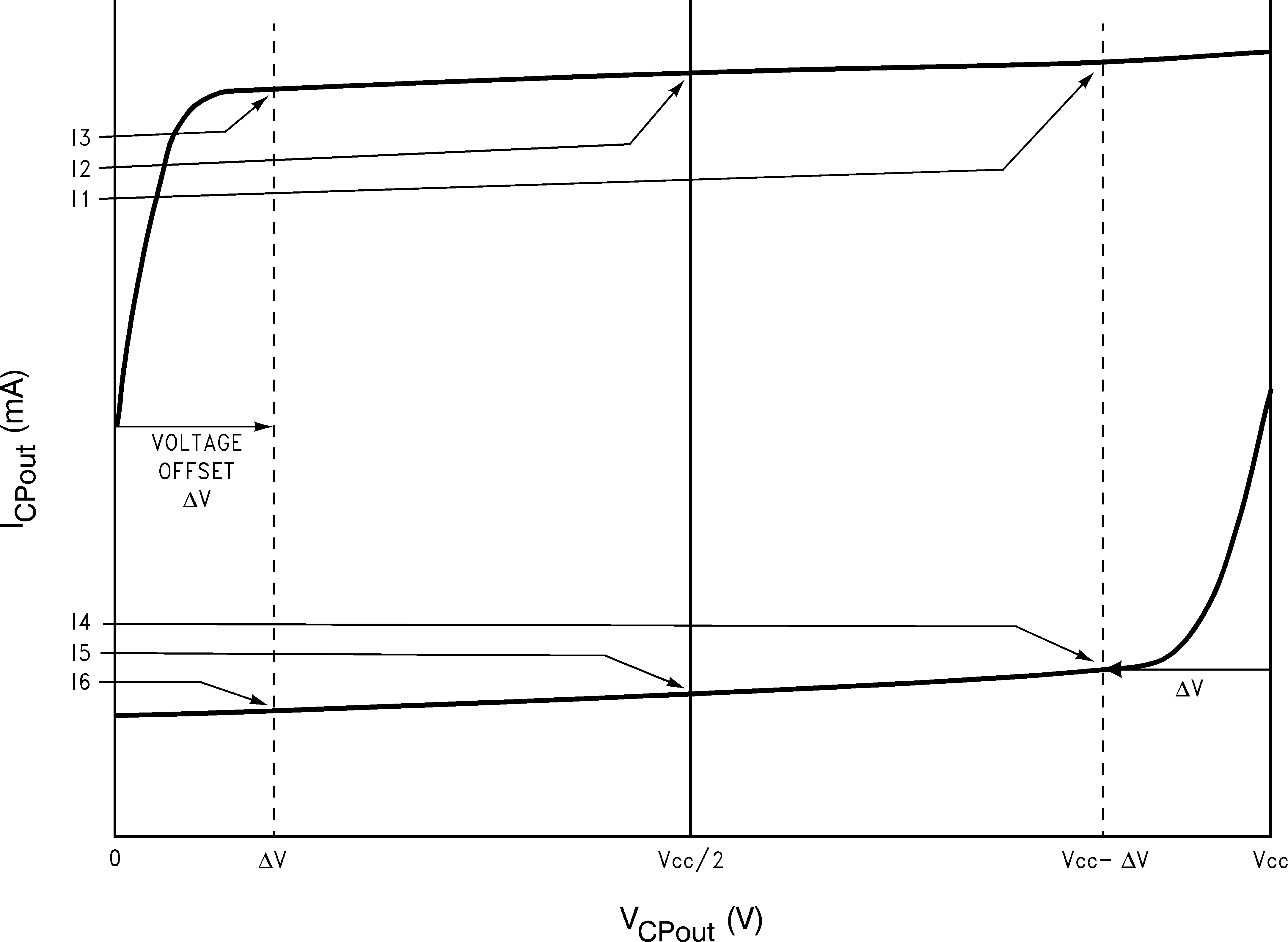
7.1.1 Charge Pump Output Current Magnitude Variation Vs. Charge Pump Output Voltage
7.1.2 Charge Pump Sink Current Vs. Charge Pump Output Source Current Mismatch

7.2 Differential Voltage Measurement Terminology
The differential voltage of a differential signal can be described by two different definitions causing confusion when reading datasheets or communicating with other engineers. This section will address the measurement and description of a differential signal so that the reader will be able to understand and discern between the two different definitions when used.
The first definition used to describe a differential signal is the absolute value of the voltage potential between the inverting and non-inverting signal. The symbol for this first measurement is typically VID or VOD depending on if an input or output voltage is being described.
The second definition used to describe a differential signal is to measure the potential of the non-inverting signal with respect to the inverting signal. The symbol for this second measurement is VSS and is a calculated parameter. Nowhere in the IC does this signal exist with respect to ground, it only exists in reference to its differential pair. VSS can be measured directly by oscilloscopes with floating references, otherwise this value can be calculated as twice the value of VOD as described in the first description.
Figure 4 illustrates the two different definitions side-by-side for inputs and Figure 5 illustrates the two different definitions side-by-side for outputs. The VID and VOD definitions show VA and VB DC levels that the non-inverting and inverting signals toggle between with respect to ground. VSS input and output definitions show that if the inverting signal is considered the voltage potential reference, the non-inverting signal voltage potential is now increasing and decreasing above and below the non-inverting reference. Thus the peak-to-peak voltage of the differential signal can be measured.
VID and VOD are often defined as volts (V) and VSS is often defined as volts peak-to-peak (VPP).
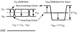 Figure 4. Two Different Definitions for Differential Input Signals
 Figure 5. Two Different Definitions for Differential Output Signals
Refer to Application Note AN-912, Common Data Transmission Parameters and their Definitions (SNLA036) for more information.