SNAS489K March   2011  – December 2014 LMK04803 , LMK04805 , LMK04806 , LMK04808

PRODUCTION DATA.  

  1. Features
  2. Applications
  3. Description
  4. Revision History
  5. Pin Configuration and Functions
  6. Specifications
    1. 6.1 Absolute Maximum Ratings
    2. 6.2 ESD Ratings
    3. 6.3 Recommended Operating Conditions
    4. 6.4 Thermal Information
    5. 6.5 Electrical Characteristics
    6. 6.6 Timing Requirements
    7. 6.7 Typical Characteristics: Clock Output AC Characteristics
  7. Parameter Measurement Information
    1. 7.1 Charge Pump Current Specification Definitions
      1. 7.1.1 Charge Pump Output Current Magnitude Variation Vs. Charge Pump Output Voltage
      2. 7.1.2 Charge Pump Sink Current Vs. Charge Pump Output Source Current Mismatch
      3. 7.1.3 Charge Pump Output Current Magnitude Variation vs. Ambient Temperature"Temperature" to "Ambient Temperature" in heading titled "Charge Pump Output Current Magnitude Variation vs. Ambient Temperature"
    2. 7.2 Differential Voltage Measurement Terminology
  8. Detailed Description
    1. 8.1 Overview
      1. 8.1.1  System Architecture
      2. 8.1.2  PLL1 Redundant Reference Inputs (CLKin0/CLKin0* and CLKin1/CLKin1*)
      3. 8.1.3  PLL1 Tunable Crystal Support
      4. 8.1.4  VCXO/CRYSTAL Buffered Outputs
      5. 8.1.5  Frequency Holdover
      6. 8.1.6  Integrated Loop Filter Poles
      7. 8.1.7  Internal VCO
      8. 8.1.8  External VCO Mode
      9. 8.1.9  Clock Distribution
        1. 8.1.9.1 CLKout DIVIDER
        2. 8.1.9.2 CLKout Delay
        3. 8.1.9.3 Programmable Output Type
        4. 8.1.9.4 Clock Output Synchronization
      10. 8.1.10 0-Delay
      11. 8.1.11 Default Startup Clocks
      12. 8.1.12 Status Pins
      13. 8.1.13 Register Readback
    2. 8.2 Functional Block Diagram
    3. 8.3 Feature Description
      1. 8.3.1  Serial MICROWIRE Timing Diagram
      2. 8.3.2  Advanced MICROWIRE Timing Diagrams
        1. 8.3.2.1 Three Extra Clocks or Double Program
        2. 8.3.2.2 Three Extra Clocks with LEuWire High
        3. 8.3.2.3 Readback
      3. 8.3.3  Inputs / Outputs
        1. 8.3.3.1 PLL1 Reference Inputs (CLKin0 and CLKin1)
        2. 8.3.3.2 PLL2 OSCin / OSCin* Port
        3. 8.3.3.3 Crystal Oscillator
      4. 8.3.4  Input Clock Switching
        1. 8.3.4.1 Input Clock Switching - Manual Mode
        2. 8.3.4.2 Input Clock Switching - Pin Select Mode
          1. 8.3.4.2.1 Pin Select Mode and Host
          2. 8.3.4.2.2 Switch Event without Holdover
          3. 8.3.4.2.3 Switch Event with Holdover
        3. 8.3.4.3 Input Clock Switching - Automatic Mode
          1. 8.3.4.3.1 Starting Active Clock
          2. 8.3.4.3.2 Clock Switch Event: PLL1 DLD
          3. 8.3.4.3.3 Clock Switch Event: PLL1 Vtune Rail
          4. 8.3.4.3.4 Clock Switch Event with Holdover
        4. 8.3.4.4 Input Clock Switching - Automatic Mode with Pin Select
          1. 8.3.4.4.1 Starting Active Clock
          2. 8.3.4.4.2 Clock Switch Event: PLL1 DLD
          3. 8.3.4.4.3 Clock Switch Event: PLL1 Vtune Rail
          4. 8.3.4.4.4 Clock Switch Event with Holdover -- revised text in Clock Switch Event with Holdover section
      5. 8.3.5  Holdover Mode
        1. 8.3.5.1 Enable Holdover
        2. 8.3.5.2 Entering Holdover
        3. 8.3.5.3 During Holdover
        4. 8.3.5.4 Exiting Holdover
        5. 8.3.5.5 Holdover Frequency Accuracy and DAC Performance
        6. 8.3.5.6 Holdover Mode - Automatic Exit of Holdover
      6. 8.3.6  PLLs
        1. 8.3.6.1 PLL1
        2. 8.3.6.2 PLL2
          1. 8.3.6.2.1 PLL2 Frequency Doubler
        3. 8.3.6.3 Digital Lock Detect
      7. 8.3.7  Status Pins
        1. 8.3.7.1 Logic Low
        2. 8.3.7.2 Digital Lock Detect
        3. 8.3.7.3 Holdover Status
        4. 8.3.7.4 DAC
        5. 8.3.7.5 PLL Divider Outputs
        6. 8.3.7.6 CLKinX_LOS
        7. 8.3.7.7 CLKinX Selected
        8. 8.3.7.8 MICROWIRE Readback
      8. 8.3.8  VCO
      9. 8.3.9  Clock Distribution
        1. 8.3.9.1 Fixed Digital Delay
        2. 8.3.9.2 Fixed Digital Delay - Example
        3. 8.3.9.3 Clock Output Synchronization (SYNC)
          1. 8.3.9.3.1 Effect of SYNC
          2. 8.3.9.3.2 Methods of Generating SYNC
          3. 8.3.9.3.3 Avoiding Clock Output Interruption Due to Sync
          4. 8.3.9.3.4 SYNC Timing
          5. 8.3.9.3.5 Dynamically Programming Digital Delay
            1. 8.3.9.3.5.1 Absolute vs. Relative Dynamic Digital Delay
            2. 8.3.9.3.5.2 Dynamic Digital Delay and 0-Delay Mode
            3. 8.3.9.3.5.3 SYNC and Minimum Step Size
            4. 8.3.9.3.5.4 Programming Overview
            5. 8.3.9.3.5.5 Internal Dynamic Digital Delay Timing
            6. 8.3.9.3.5.6 Other Timing Requirements
            7. 8.3.9.3.5.7 Absolute Dynamic Digital Delay
              1. 8.3.9.3.5.7.1 Absolute Dynamic Digital Delay - Example
            8. 8.3.9.3.5.8 Relative Dynamic Digital Delay
              1. 8.3.9.3.5.8.1 Relative Dynamic Digital Delay - Example
      10. 8.3.10 0-Delay Mode
    4. 8.4 Device Functional Modes
      1. 8.4.1 Mode Selection
      2. 8.4.2 Operating Modes
        1. 8.4.2.1 Dual PLL
        2. 8.4.2.2 0-Delay Dual PLL
        3. 8.4.2.3 Single PLL
        4. 8.4.2.4 0-Delay Single PLL
        5. 8.4.2.5 Clock Distribution
        6. 8.4.2.6 Mode 15 Additional Configurations
    5. 8.5 Programming
      1. 8.5.1 Special Programming Case for R0 to R5 for CLKoutX_Y_DIV and CLKoutX_Y_DDLY
        1. 8.5.1.1 Example
      2. 8.5.2 Recommended Programming Sequence
        1. 8.5.2.1 Overview
      3. 8.5.3 Readback
        1. 8.5.3.1 Readback - Example
    6. 8.6 Register Maps
      1. 8.6.1 Register Map and Readback Register Map
      2. 8.6.2 Default Device Register Settings After Power On Reset
      3. 8.6.3 Register Descriptions
        1. 8.6.3.1  Register R0 TO R5
          1. 8.6.3.1.1 CLKoutX_Y_PD, Powerdown CLKoutX_Y Output Path
          2. 8.6.3.1.2 CLKoutX_Y_OSCin_Sel, Clock Group Source
          3. 8.6.3.1.3 CLKoutY_ADLY_SEL[29], CLKoutX_ADLY_SEL[28], Select Analog Delay
          4. 8.6.3.1.4 CLKoutX_Y_DDLY, Clock Channel Digital Delay
          5. 8.6.3.1.5 Reset
          6. 8.6.3.1.6 POWERDOWN
          7. 8.6.3.1.7 CLKoutX_Y_HS, Digital Delay Half Shift
          8. 8.6.3.1.8 CLKoutX_Y_DIV, Clock Output Divide
        2. 8.6.3.2  Registers R6 TO R8
          1. 8.6.3.2.1 CLKoutX_TYPE
          2. 8.6.3.2.2 CLKoutX_Y_ADLY
        3. 8.6.3.3  Register R10
          1. 8.6.3.3.1  OSCout1_LVPECL_AMP, LVPECL Output Amplitude Control
          2. 8.6.3.3.2  OSCout0_TYPE
          3. 8.6.3.3.3  EN_OSCoutX, OSCout Output Enable
          4. 8.6.3.3.4  OSCoutX_MUX, Clock Output Mux
          5. 8.6.3.3.5  PD_OSCin, OSCin Powerdown Control
          6. 8.6.3.3.6  OSCout_DIV, Oscillator Output Divide
          7. 8.6.3.3.7  VCO_MUX
          8. 8.6.3.3.8  EN_FEEDBACK_MUX
          9. 8.6.3.3.9  VCO_DIV, VCO Divider
          10. 8.6.3.3.10 FEEDBACK_MUX
        4. 8.6.3.4  Register R11
          1. 8.6.3.4.1 MODE: Device Mode
          2. 8.6.3.4.2 EN_SYNC, Enable Synchronization
          3. 8.6.3.4.3 NO_SYNC_CLKoutX_Y
          4. 8.6.3.4.4 SYNC_MUX
          5. 8.6.3.4.5 SYNC_QUAL
          6. 8.6.3.4.6 SYNC_POL_INV
          7. 8.6.3.4.7 SYNC_EN_AUTO
          8. 8.6.3.4.8 SYNC_TYPE
          9. 8.6.3.4.9 EN_PLL2_XTAL
        5. 8.6.3.5  Register R12
          1. 8.6.3.5.1 LD_MUX
          2. 8.6.3.5.2 LD_TYPE
          3. 8.6.3.5.3 SYNC_PLLX_DLD
          4. 8.6.3.5.4 EN_TRACK
          5. 8.6.3.5.5 HOLDOVER_MODE
        6. 8.6.3.6  Register R13
          1. 8.6.3.6.1 HOLDOVER_MUX
          2. 8.6.3.6.2 HOLDOVER_TYPE
          3. 8.6.3.6.3 Status_CLKin1_MUX
          4. 8.6.3.6.4 Status_CLKin0_TYPE
          5. 8.6.3.6.5 DISABLE_DLD1_DET
          6. 8.6.3.6.6 Status_CLKin0_MUX
          7. 8.6.3.6.7 CLKin_SELECT_MODE
          8. 8.6.3.6.8 CLKin_Sel_INV
          9. 8.6.3.6.9 EN_CLKinX
        7. 8.6.3.7  Register 14
          1. 8.6.3.7.1 LOS_TIMEOUT
          2. 8.6.3.7.2 EN_LOS
          3. 8.6.3.7.3 Status_CLKin1_TYPE
          4. 8.6.3.7.4 CLKinX_BUF_TYPE, PLL1 CLKinX/CLKinX* Buffer Type
          5. 8.6.3.7.5 DAC_HIGH_TRIP
          6. 8.6.3.7.6 DAC_LOW_TRIP
          7. 8.6.3.7.7 EN_VTUNE_RAIL_DET
        8. 8.6.3.8  REGISTER 15
          1. 8.6.3.8.1 MAN_DAC
          2. 8.6.3.8.2 EN_MAN_DAC
          3. 8.6.3.8.3 HOLDOVER_DLD_CNT
          4. 8.6.3.8.4 FORCE_HOLDOVER
        9. 8.6.3.9  Register 16
          1. 8.6.3.9.1 XTAL_LVL
        10. 8.6.3.10 Register 23
          1. 8.6.3.10.1 DAC_CNT
        11. 8.6.3.11 Register 24
          1. 8.6.3.11.1 PLL2_C4_LF, PLL2 Integrated Loop Filter Component
          2. 8.6.3.11.2 PLL2_C3_LF, PLL2 Integrated Loop Filter Component
          3. 8.6.3.11.3 PLL2_R4_LF, PLL2 Integrated Loop Filter Component
          4. 8.6.3.11.4 PLL2_R3_LF, PLL2 Integrated Loop Filter Component
          5. 8.6.3.11.5 PLL1_N_DLY
          6. 8.6.3.11.6 PLL1_R_DLY
          7. 8.6.3.11.7 PLL1_WND_SIZE
        12. 8.6.3.12 Register 25
          1. 8.6.3.12.1 DAC_CLK_DIV
          2. 8.6.3.12.2 PLL1_DLD_CNT
        13. 8.6.3.13 Register 26
          1. 8.6.3.13.1 PLL2_WND_SIZE
          2. 8.6.3.13.2 EN_PLL2_REF_2X, PLL2 Reference Frequency Doubler
          3. 8.6.3.13.3 PLL2_CP_POL, PLL2 Charge Pump Polarity
          4. 8.6.3.13.4 PLL2_CP_GAIN, PLL2 Charge Pump Current
          5. 8.6.3.13.5 PLL2_DLD_CNT
          6. 8.6.3.13.6 PLL2_CP_TRI, PLL2 Charge Pump TRI-STATE
        14. 8.6.3.14 REGISTER 27
          1. 8.6.3.14.1 PLL1_CP_POL, PLL1 Charge Pump Polarity
          2. 8.6.3.14.2 PLL1_CP_GAIN, PLL1 Charge Pump Current
          3. 8.6.3.14.3 CLKinX_PreR_DIV
          4. 8.6.3.14.4 PLL1_R, PLL1 R Divider
          5. 8.6.3.14.5 PLL1_CP_TRI, PLL1 Charge Pump TRI-STATE
        15. 8.6.3.15 Register 28
          1. 8.6.3.15.1 PLL2_R, PLL2 R Divider
          2. 8.6.3.15.2 PLL1_N, PLL1 N Divider
        16. 8.6.3.16 Register 29
          1. 8.6.3.16.1 OSCin_FREQ, PLL2 Oscillator Input Frequency Register
          2. 8.6.3.16.2 PLL2_FAST_PDF, High PLL2 Phase Detector Frequency
          3. 8.6.3.16.3 PLL2_N_CAL, PLL2 N Calibration Divider
        17. 8.6.3.17 Register 30
          1. 8.6.3.17.1 PLL2_P, PLL2 N Prescaler Divider
          2. 8.6.3.17.2 PLL2_N, PLL2 N Divider
        18. 8.6.3.18 Register 31
          1. 8.6.3.18.1 READBACK_LE
          2. 8.6.3.18.2 READBACK_ADDR
          3. 8.6.3.18.3 uWire_LOCK
  9. Application and Implementation
    1. 9.1 Application Information
      1. 9.1.1 Loop Filter
        1. 9.1.1.1 PLL1
        2. 9.1.1.2 PLL2
      2. 9.1.2 Driving CLKin and OSCin Inputs
        1. 9.1.2.1 Driving CLKin Pins with a Differential Source
        2. 9.1.2.2 Driving CLKin Pins with a Single-Ended Source
      3. 9.1.3 Termination and Use of Clock Output (Drivers)
        1. 9.1.3.1 Termination for DC Coupled Differential Operation
        2. 9.1.3.2 Termination for AC Coupled Differential Operation
        3. 9.1.3.3 Termination for Single-Ended Operation
      4. 9.1.4 Frequency Planning with the LMK0480x Family
      5. 9.1.5 PLL Programming
        1. 9.1.5.1 Example PLL2 N Divider Programming
          1. 9.1.5.1.1 Example PLL2 N Divider Programming
      6. 9.1.6 Digital Lock Detect Frequency Accuracy
        1. 9.1.6.1 Minimum Digital Lock Detect Time Calculation Example
      7. 9.1.7 Calculating Dynamic Digital Delay Values for any Divide
        1. 9.1.7.1 Example
      8. 9.1.8 Optional Crystal Oscillator Implementation (OSCin/OSCin*)
      9. 9.1.9 Application Curves
    2. 9.2 Typical Applications
      1. 9.2.1 Design Requirements
      2. 9.2.2 Detailed Design Procedure
        1. 9.2.2.1 Device Selection
          1. 9.2.2.1.1 Clock Architect
          2. 9.2.2.1.2 Clock Design Tool
          3. 9.2.2.1.3 Calculation Using LCM
        2. 9.2.2.2 Device Configuration
          1. 9.2.2.2.1 PLL LO Reference
          2. 9.2.2.2.2 POR Clock
        3. 9.2.2.3 PLL Loop Filter Design
          1. 9.2.2.3.1 PLL1 Loop Filter Design
          2. 9.2.2.3.2 PLL2 Loop Filter Design
        4. 9.2.2.4 Clock Output Assignment
        5. 9.2.2.5 Other Device Specific Configuration
          1. 9.2.2.5.1 Digital Lock Detect
          2. 9.2.2.5.2 Holdover
        6. 9.2.2.6 Device Programming
      3. 9.2.3 Application Curve
    3. 9.3 System Examples
      1. 9.3.1 System Level Diagram
    4. 9.4 Do's and Don'ts
      1. 9.4.1 LVCMOS Complementary vs. Non-Complementary Operation
      2. 9.4.2 LVPECL Outputs
  10. 10Power Supply Recommendations
    1. 10.1 Pin Connection Recommendations
      1. 10.1.1 Vcc Pins and Decoupling
        1. 10.1.1.1 Vcc2, Vcc3, Vcc10, Vcc11, Vcc12, Vcc13 (CLKout Vccs)
        2. 10.1.1.2 Vcc1 (VCO), Vcc4 (Digital), and Vcc9 (PLL2)
        3. 10.1.1.3 Vcc6 (PLL1 Charge Pump) and Vcc8 (PLL2 Charge Pump)
        4. 10.1.1.4 Vcc5 (CLKin and OSCout1), Vcc7 (OSCin and OSCout0)
      2. 10.1.2 LVPECL Outputs
      3. 10.1.3 Unused Clock Outputs
      4. 10.1.4 Unused Clock Inputs
      5. 10.1.5 LDO Bypass
    2. 10.2 Current Consumption and Power Dissipation Calculations
  11. 11Layout
    1. 11.1 Layout Guidelines
    2. 11.2 Layout Example
  12. 12Device and Documentation Support
    1. 12.1 Device Support
      1. 12.1.1 Development Support
    2. 12.2 Documentation Support
      1. 12.2.1 Related Documentation
    3. 12.3 Related Links
    4. 12.4 Trademarks
    5. 12.5 Electrostatic Discharge Caution
    6. 12.6 Glossary
  13. 13Mechanical, Packaging, and Orderable Information

Package Options

Mechanical Data (Package|Pins)
Thermal pad, mechanical data (Package|Pins)
Orderable Information

11 Layout

11.1 Layout Guidelines

Power consumption of the LMK0480x family of devices can be high enough to require attention to thermal management. For reliability and performance reasons the die temperature should be limited to a maximum of 125 °C. That is, as an estimate, TA (ambient temperature) plus device power consumption times RθJA should not exceed 125 °C.

The package of the device has an exposed pad that provides the primary heat removal path as well as excellent electrical grounding to a printed circuit board. To maximize the removal of heat from the package a thermal land pattern including multiple vias to a ground plane must be incorporated on the PCB within the footprint of the package. The exposed pad must be soldered down to ensure adequate heat conduction out of the package.

A recommended land and via pattern is shown in Figure 41. More information on soldering WQFN packages can be obtained from www.ti.com/packaging/. See also the packaging information in Mechanical, Packaging, and Orderable Information.

To minimize junction temperature, it is recommended that a simple heat sink be built into the PCB (if the ground plane layer is not exposed). This is done by including a copper area on the opposite side of the PCB from the device. This copper area may be plated or solder coated to prevent corrosion, but should not have conformal coating (if possible), which could provide thermal insulation. The vias shown in Figure 41 should connect these top and bottom copper layers and to the ground layer. These vias act as “heat pipes” to carry the thermal energy away from the device side of the board to where it can be more effectively dissipated. Avoid routing traces close to exposed ground pad to ensure proper thermal flow on the PCB.

30102373.gif
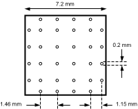
Figure 41. Recommended Land and Via Pattern

11.2 Layout Example

layout_snas645.gif
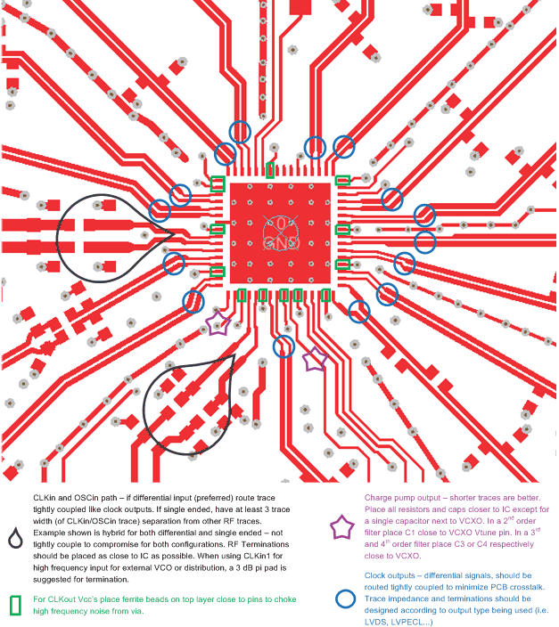
Figure 42. LMK0480x Layout Example