SNAS814A December 2020 – January 2022 LMK1C1106 , LMK1C1108
PRODUCTION DATA
- 1 Features
- 2 Applications
- 3 Description
- 4 Revision History
- 5 Pin Configuration and Functions
- 6 Specifications
- 7 Parameter Measurement Information
- 8 Detailed Description
- 9 Application and Implementation
- 10Power Supply Recommendations
- 11Layout
- 12Device and Documentation Support
- 13Mechanical, Packaging, and Orderable Information
Package Options
Mechanical Data (Package|Pins)
- PW|16
Thermal pad, mechanical data (Package|Pins)
Orderable Information
3 Description
The LMK1C110x is a modular, high-performance, low-skew, general-purpose clock buffer family from Texas Instruments. The entire family is designed with a modular approach in mind. Five different fan-out variations, 1:2, 1:3, 1:4, 1:6 and 1:8 are available.
All of the devices within this family are pin-compatible to each other and backwards compatible to the CDCLVC110x family for easy handling.
All family members share the same high performing characteristics such as low additive jitter, low skew, and wide operating temperature range.
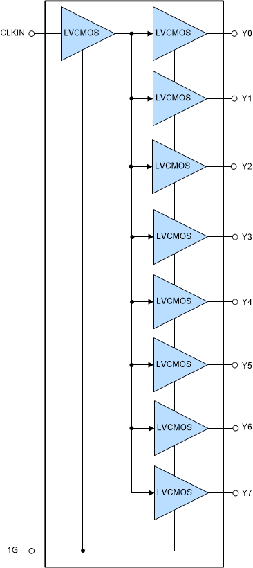
The LMK1C110x supports a synchronous output enable control (1G) which switches the outputs into a low state when 1G is low. These devices have a fail-safe input that prevents oscillation at the outputs in the absence of an input signal and allows for input signals before VDD is supplied.
The LMK1C110x family operates in a 1.8-V, 2.5-V and 3.3-V environment and are characterized for operation from –40°C to 125°C.
| PART NUMBER | PACKAGE | BODY SIZE (NOM) |
|---|---|---|
| LMK1C1106 | TSSOP (14) | 5.00 mm x 4.40 mm |
| LMK1C1108 | TSSOP (16) | 5.00 mm x 4.40 mm |
 Functional Block Diagram