SNOSCX0A June 2013 – December 2014 LMP92064
PRODUCTION DATA.
- 1 Features
- 2 Applications
- 3 Description
- 4 Revision History
- 5 Pin Configuration and Functions
- 6 Specifications
- 7 Detailed Description
- 8 Application and Implementation
- 9 Power Supply Recommendations
- 10Layout
- 11Device and Documentation Support
- 12Mechanical, Packaging, and Orderable Information
Package Options
Mechanical Data (Package|Pins)
- NHR|16
Thermal pad, mechanical data (Package|Pins)
Orderable Information
1 Features
- Two Simultaneous Sampling 12-Bit ADCs
- Conversion Rate: 125 kSps (Minimum)
- 12-Bit Current Sense Channel
- Input-referred Offset: ±15 μV
- Common-mode Voltage Range: –0.2 V to 2 V
- Maximum Differential Input Voltage: 75 mV
- Fixed Gain: 25 V/V
- Gain Error: ±0.75% (Maximum)
- Bandwidth (–3dB): 70 kHz
- DC PSRR: 100 dB
- DC CMRR: 110 dB
- 12-Bit Voltage Channel
- INL: ±1 LSB
- Offset Error: ±2 mV (Maximum)
- Gain Error: ±0.75% (Maximum)
- Maximum Input Voltage: 2.048 V
- Bandwidth: 100 kHz
- Internal Reference
- SPI Frequency: Up to 20 MHz
- Temperature Range: –40°C to 105°C
- 16-Pin WSON Package
2 Applications
- Enterprise Servers
- Telecommunications
- Power Management
3 Description
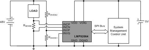
The LMP92064 is a precision low-side digital current sensor and voltage monitor with a digital SPI interface. This analog frontend (AFE) includes a precision current sense amplifier to measure a load current across a shunt resistor and a buffered voltage channel to measure the voltage supply of the load. The current and voltage channels are sampled simultaneously by independent 125-kSps, 12-bit ADC converters, allowing for very accurate power calculations in unidirectional sensing applications.
The LMP92064 includes an internal 2.048-V reference for the ADCs, eliminating the need of an external reference and reducing component count and board space.
A host can communicate with the LMP92064 using a four-wire SPI interface running at speeds of up to
20 MHz. The fast SPI interface lets the user take advantage of the higher bandwidth ADC to capture fast varying signals. The four-wire interface with dedicated unidirectional input and output lines also allows for an easy interface to digital isolators in applications where isolation is required.
The LMP92064 operates from a single 4.5-V to 5.5-V supply and includes a separate digital supply pin. The LMP92064 is specified over a temperature range of –40°C to 105°C, and is available in a 5-mm x 4-mm 16-Pin WSON package.
Device Information(1)
| PART NUMBER | PACKAGE | BODY SIZE (NOM) |
|---|---|---|
| LMP92064 | WSON (16) | 5.00 mm x 4.00 mm |
- For all available packages, see the orderable addendum at the end of the datasheet.
Simplified Schematic