SNOSCX0A June 2013 – December 2014 LMP92064
PRODUCTION DATA.
- 1 Features
- 2 Applications
- 3 Description
- 4 Revision History
- 5 Pin Configuration and Functions
- 6 Specifications
- 7 Detailed Description
- 8 Application and Implementation
- 9 Power Supply Recommendations
- 10Layout
- 11Device and Documentation Support
- 12Mechanical, Packaging, and Orderable Information
Package Options
Mechanical Data (Package|Pins)
- NHR|16
Thermal pad, mechanical data (Package|Pins)
Orderable Information
5 Pin Configuration and Functions
WSON Package
16 Pins
Top View
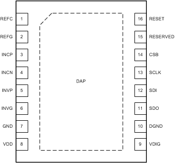
Pin Functions
| PIN | I/O(1) | DESCRIPTION | |
|---|---|---|---|
| NAME | NO. | ||
| REFC | 1 | — | Internal reference bypass capacitor pin |
| REFG | 2 | G | Internal reference ground |
| INCP | 3 | I | Positive current channel input |
| INCN | 4 | I | Negative current channel input |
| INVP | 5 | I | Positive voltage channel input |
| INVG | 6 | G | Ground reference for the negative voltage channel input |
| GND | 7 | G | Analog ground |
| VDD | 8 | P | Analog power supply |
| VDIG | 9 | P | Digital power supply |
| DGND | 10 | G | Digital ground |
| SDO | 11 | O | SPI Bus push-pull serial data digital output |
| SDI | 12 | I | SPI Bus serial data digital input |
| SCLK | 13 | I | SPI Bus clock digital input |
| CSB | 14 | I | SPI Bus chip select bar digital input |
| RESERVED | 15 | — | Reserved (Do not connect) |
| RESET | 16 | I | Reset (high-active) |
| DAP | n/a | — | No connection (Do not connect) |
(1) G = Ground, I = Input, O = Output, P = Power