SNOSCX0A June 2013 – December 2014 LMP92064
PRODUCTION DATA.
- 1 Features
- 2 Applications
- 3 Description
- 4 Revision History
- 5 Pin Configuration and Functions
- 6 Specifications
- 7 Detailed Description
- 8 Application and Implementation
- 9 Power Supply Recommendations
- 10Layout
- 11Device and Documentation Support
- 12Mechanical, Packaging, and Orderable Information
Package Options
Mechanical Data (Package|Pins)
- NHR|16
Thermal pad, mechanical data (Package|Pins)
Orderable Information
10 Layout
10.1 Layout Guidelines
- Connect the sense resistor pads directly to the INCP and INCN inputs of the LMP92064 using “Kelvin” or “4-wire” connection techniques. See the Current Input Error Sources and Layout Considerations section for more information.
- Bypass capacitors should be placed in close proximity to the supply pins. It is recommended to use a 0.1-μF capacitor on each supply pin. Additional bypass capacitors can be used.
- A 1-μF ceramic bypass capacitor should be placed in close proximity to the REFC pin.
- The SPI signals traces should be routed close together.
- Series resistors should be placed at the SPI sources.
10.1.1 Current Input Error Sources
The traces leading to and from the sense resistor can be significant error sources. With small value sense resistors (<100 mΩ), trace resistance shared with the load can cause significant errors. TI recommends connecting the sense resistor pads directly to the INCP and INCN inputs of the LMP92064 using “Kelvin” or “4-wire” connection techniques. An example is shown in Figure 28.
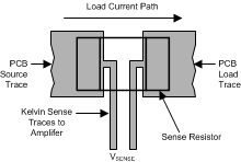 Figure 28. 4-Wire "Kelvin" Sensing Technique
Because the sense traces only carry the amplifier bias current, the connecting input traces can be thinner, signal level traces. The traces should be one continuous piece of copper from the sense resistor pad to the LMP92064 input pin pad, and ideally on the same layer with minimal vias or connectors. This can be important around the sense resistor if it is generating any significant heat. To minimize noise pickup and thermal errors, the input traces should be treated as a signal pair and routed tightly together with a direct path to the input pins. The input traces should be run away from noise sources, such as digital lines, switching supplies or motor drive lines.
10.2 Layout Example
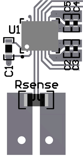 Figure 29. Layout Schematic