SNVSBP4C March 2020 – January 2021 LMQ61460-Q1
PRODUCTION DATA
- 1 Features
- 2 Applications
- 3 Description
- 4 Revision History
- 5 Description (continued)
- 6 Device Comparison Table
- 7 Pin Configuration and Functions
- 8 Specifications
-
9 Detailed Description
- 9.1 Overview
- 9.2 Functional Block Diagram
- 9.3
Feature Description
- 9.3.1 EN/SYNC Uses for Enable and VIN UVLO
- 9.3.2 EN/SYNC Pin Uses for Synchronization
- 9.3.3 Adjustable Switching Frequency
- 9.3.4 Clock Locking
- 9.3.5 PGOOD Output Operation
- 9.3.6 Internal LDO, VCC UVLO, and BIAS Input
- 9.3.7 Bootstrap Voltage and VCBOOT-UVLO (CBOOT Pin)
- 9.3.8 Adjustable SW Node Slew Rate
- 9.3.9 Spread Spectrum
- 9.3.10 Soft Start and Recovery From Dropout
- 9.3.11 Output Voltage Setting
- 9.3.12 Overcurrent and Short Circuit Protection
- 9.3.13 Thermal Shutdown
- 9.3.14 Input Supply Current
- 9.4 Device Functional Modes
-
10Application and Implementation
- 10.1 Application Information
- 10.2
Typical Application
- 10.2.1 Design Requirements
- 10.2.2
Detailed Design Procedure
- 10.2.2.1 Choosing the Switching Frequency
- 10.2.2.2 Setting the Output Voltage
- 10.2.2.3 Inductor Selection
- 10.2.2.4 Output Capacitor Selection
- 10.2.2.5 Input Capacitor Selection
- 10.2.2.6 BOOT Capacitor
- 10.2.2.7 BOOT Resistor
- 10.2.2.8 VCC
- 10.2.2.9 BIAS
- 10.2.2.10 CFF and RFF Selection
- 10.2.2.11 External UVLO
- 10.2.3 Application Curves
- 11Power Supply Recommendations
- 12Layout
- 13Device and Documentation Support
- 14Mechanical, Packaging, and Orderable Information
Package Options
Mechanical Data (Package|Pins)
- RJR|14
Thermal pad, mechanical data (Package|Pins)
Orderable Information
9.3.1 EN/SYNC Uses for Enable and VIN UVLO
Start-up and shutdown are controlled by the EN/SYNC input and VIN UVLO. For the device to remain in shutdown mode, apply a voltage below VEN_WAKE (.4 V) to the EN pin. In shutdown mode, the quiescent current drops to 0.6 µA (typical). At a voltage above VEN_WAKE and below VEN, VCC is active and the SW node is inactive. Once the EN voltage is above VEN, the chip begins to switch normally provided the input voltage is above 3 V.
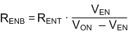
The EN/SYNC pin cannot be left floating. The simplest way to enable the operation is to connect the EN/SYNC pin to VIN, allowing self-start-up of the device when VIN drives the internal VCC above its UVLO level. However, many applications benefit from the employment of an enable divider network as shown in Figure 9-1, which establishes a precision input undervoltage lockout (UVLO). This can be used for sequencing, preventing re-triggering the device when used with long input cables, or reducing the occurrence of deep discharge of a battery power source. Note that the precision enable threshold VEN has a 8.1% tolerance. Hysteresis must be enough to prevent re-triggering. External logic output of another IC can also be used to drive the EN/SYNC pin, allowing system power sequencing.
 Figure 9-1 VIN SYNC Using the EN
pin
Figure 9-1 VIN SYNC Using the EN
pinResistor values can be calculated using Equation 1.
where
- VON is the desired typical start-up input voltage for the circuit being designed
Note that since the EN pin can also be used as an external synchronization clock input. A blanking time, tB, is applied to the enable logic after a clock edge is detected. Any logic change within the blanking time is ignored. Blanking time is not applied when the device is in shutdown mode. The blanking time ranges from 4 µs to 28 µs. To effectively disable the output, the EN/SYNC input must stay low for longer than 28 µs.