SNVSAV8B June 2017 – August 2020 LMR23615
PRODUCTION DATA
- 1 Features
- 2 Applications
- 3 Description
- 4 Revision History
- 5 Pin Configuration and Functions
- 6 Specifications
-
7 Detailed Description
- 7.1 Overview
- 7.2 Functional Block Diagram
- 7.3
Feature Description
- 7.3.1 Fixed-Frequency, Peak-Current-Mode Control
- 7.3.2 Adjustable Frequency
- 7.3.3 Adjustable Output Voltage
- 7.3.4 Enable/Sync
- 7.3.5 VCC, UVLO
- 7.3.6 Minimum ON-Time, Minimum-OFF Time, and Frequency Foldback at Dropout Conditions
- 7.3.7 Internal Compensation and CFF
- 7.3.8 Bootstrap Voltage (BOOT)
- 7.3.9 Overcurrent and Short-Circuit Protection
- 7.3.10 Thermal Shutdown
- 7.4 Device Functional Modes
-
8 Application and Implementation
- 8.1 Application Information
- 8.2
Typical Applications
- 8.2.1 Design Requirements
- 8.2.2
Detailed Design Procedure
- 8.2.2.1 Custom Design With WEBENCH® Tools
- 8.2.2.2 Output Voltage Setpoint
- 8.2.2.3 Switching Frequency
- 8.2.2.4 Inductor Selection
- 8.2.2.5 Output Capacitor Selection
- 8.2.2.6 Feedforward Capacitor
- 8.2.2.7 Input Capacitor Selection
- 8.2.2.8 Bootstrap Capacitor Selection
- 8.2.2.9 VCC Capacitor Selection
- 8.2.2.10 Undervoltage Lockout Setpoint
- 8.2.3 Application Curves
- 9 Power Supply Recommendations
- 10Layout
- 11Device and Documentation Support
- 12Mechanical, Packaging, and Orderable Information
Package Options
Mechanical Data (Package|Pins)
- DRR|12
Thermal pad, mechanical data (Package|Pins)
- DRR|12
Orderable Information
8.2 Typical Applications
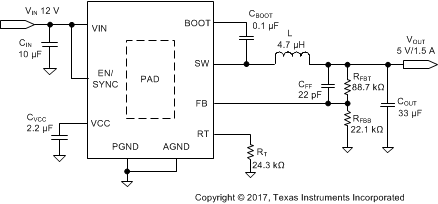
The LMR23615 only requires a few external components to convert from a wide voltage range supply to a fixed output voltage. Figure 8-1 shows a basic schematic.
 Figure 8-1 Application Circuit
The external components must fulfill the needs of the application, but also the stability criteria of the device control loop. Table 8-1 can be used to simplify the output filter component selection.
Table 8-1 L, COUT, and CFF Typical Values
| fSW (kHz) | VOUT (V) | L (µH) (1) | COUT (µF) (2) | CFF (pF)(4) | RFBT (kΩ)(3) |
|---|---|---|---|---|---|
| 200 | 3.3 | 22 | 200 | 220 | 51 |
| 5 | 33 | 150 | 120 | 88.7 | |
| 12 | 56 | 68 | See note(5) | 243 | |
| 24 | 56 | 33 | See note(5) | 510 | |
| 400 | 3.3 | 10 | 120 | 100 | 51 |
| 5 | 15 | 90 | 68 | 88.7 | |
| 12 | 33 | 47 | See note(5) | 243 | |
| 24 | 33 | 22 | See note(5) | 510 | |
| 1000 | 3.3 | 4.7 | 68 | 47 | 51 |
| 5 | 5.6 | 47 | 22 | 88.7 | |
| 12 | 10 | 33 | See note(5) | 243 | |
| 2200 | 3.3 | 2.2 | 33 | 22 | 51 |
| 5 | 3.3 | 22 | 15 | 88.7 |
(1) Inductance value is calculated based on VIN = 36 V.
(2) All the COUT values are after derating. Add more when using ceramic capacitors.
(3) RFBT = 0 Ω for VOUT = 1 V. RFBB = 22.1 kΩ for all other VOUT settings.
(4) For designs with RFBT other than recommended value, adjust CFF so that (CFF × RFBT) is unchanged and adjust RFBB such that (RFBT / RFBB) is unchanged.
(5) High ESR COUT gives enough phase boost and CFF not needed.