SNVSAV8B June 2017 – August 2020 LMR23615
PRODUCTION DATA
- 1 Features
- 2 Applications
- 3 Description
- 4 Revision History
- 5 Pin Configuration and Functions
- 6 Specifications
-
7 Detailed Description
- 7.1 Overview
- 7.2 Functional Block Diagram
- 7.3
Feature Description
- 7.3.1 Fixed-Frequency, Peak-Current-Mode Control
- 7.3.2 Adjustable Frequency
- 7.3.3 Adjustable Output Voltage
- 7.3.4 Enable/Sync
- 7.3.5 VCC, UVLO
- 7.3.6 Minimum ON-Time, Minimum-OFF Time, and Frequency Foldback at Dropout Conditions
- 7.3.7 Internal Compensation and CFF
- 7.3.8 Bootstrap Voltage (BOOT)
- 7.3.9 Overcurrent and Short-Circuit Protection
- 7.3.10 Thermal Shutdown
- 7.4 Device Functional Modes
-
8 Application and Implementation
- 8.1 Application Information
- 8.2
Typical Applications
- 8.2.1 Design Requirements
- 8.2.2
Detailed Design Procedure
- 8.2.2.1 Custom Design With WEBENCH® Tools
- 8.2.2.2 Output Voltage Setpoint
- 8.2.2.3 Switching Frequency
- 8.2.2.4 Inductor Selection
- 8.2.2.5 Output Capacitor Selection
- 8.2.2.6 Feedforward Capacitor
- 8.2.2.7 Input Capacitor Selection
- 8.2.2.8 Bootstrap Capacitor Selection
- 8.2.2.9 VCC Capacitor Selection
- 8.2.2.10 Undervoltage Lockout Setpoint
- 8.2.3 Application Curves
- 9 Power Supply Recommendations
- 10Layout
- 11Device and Documentation Support
- 12Mechanical, Packaging, and Orderable Information
Package Options
Mechanical Data (Package|Pins)
- DRR|12
Thermal pad, mechanical data (Package|Pins)
- DRR|12
Orderable Information
3 Description
The LMR23615 SIMPLE SWITCHER® is an easy-to-use 36-V, 1.5-A synchronous step-down regulator. With a wide input range from 4 V to 36 V, the device is suitable for various industrial applications for power conditioning from unregulated sources. Peak current mode control is employed to achieve simple control-loop compensation and cycle-by-cycle current limiting. A quiescent current of 75 µA makes the device suitable for battery-powered systems. An ultra-low 2-µA shutdown current can further prolong battery life. Internal loop compensation means that the user is free from the tedious task of loop-compensation design and also minimizes the external components needed. An extended family is available in 2.5-A (LMR23625) and 3-A (LMR23630) load-current options in pin-to-pin compatible packages, allowing simple, optimum PCB layout. A precision enable input allows simplification of regulator control and system power sequencing. Protection features include cycle-by-cycle current limit, hiccup-mode short-circuit protection, and thermal shutdown due to excessive power dissipation.
| PART NUMBER (1) | PACKAGE | BODY SIZE (NOM) |
|---|---|---|
| LMR23615 | WSON (12) | 3.00 mm × 3.00 mm |
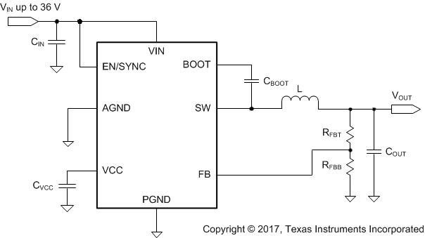
 Simplified Schematic
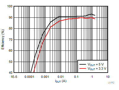
 Efficiency vs Load, VIN = 12 V