SNVSBQ5 June   2021 LMR33620AP-Q1 , LMR33630AP-Q1

PRODUCTION DATA  

  1. Features
  2. Applications
  3. Description
  4. Revision History
  5. Device Comparison Table
  6. Pin Configuration and Functions
  7. Specifications
    1. 7.1 Absolute Maximum Ratings
    2. 7.2 ESD Ratings
    3. 7.3 Recommended Operating Conditions
    4. 7.4 Thermal Information
    5. 7.5 Electrical Characteristics
    6. 7.6 Timing Characteristics
    7. 7.7 System Characteristics
    8. 7.8 Typical Characteristics
  8. Detailed Description
    1. 8.1 Overview
    2. 8.2 Functional Block Diagram
    3. 8.3 Feature Description
      1. 8.3.1 Power-Good Flag Output
      2. 8.3.2 Enable and Start-Up
      3. 8.3.3 Current Limit and Short Circuit
      4. 8.3.4 Undervoltage Lockout and Thermal Shutdown
    4. 8.4 Device Functional Modes
      1. 8.4.1 Auto Mode
      2. 8.4.2 Dropout
      3. 8.4.3 Minimum Switch On Time
  9. Application and Implementation
    1. 9.1 Application Information
    2. 9.2 Typical Application
      1. 9.2.1 Design Requirements
      2. 9.2.2 Detailed Design Procedure
        1. 9.2.2.1  Custom Design With WEBENCH® Tools
        2. 9.2.2.2  Choosing the Switching Frequency
        3. 9.2.2.3  Setting the Output Voltage
        4. 9.2.2.4  Inductor Selection
        5. 9.2.2.5  Output Capacitor Selection
        6. 9.2.2.6  Input Capacitor Selection
        7. 9.2.2.7  CBOOT
        8. 9.2.2.8  VCC
        9. 9.2.2.9  CFF Selection
        10. 9.2.2.10 External UVLO
        11. 9.2.2.11 Maximum Ambient Temperature
      3. 9.2.3 Application Curves
    3. 9.3 What to Do and What Not to Do
  10. 10Power Supply Recommendations
  11. 11Layout
    1. 11.1 Layout Guidelines
      1. 11.1.1 Ground and Thermal Considerations
    2. 11.2 Layout Example
  12. 12Device and Documentation Support
    1. 12.1 Device Support
      1. 12.1.1 Third-Party Products Disclaimer
      2. 12.1.2 Development Support
        1. 12.1.2.1 Custom Design With WEBENCH® Tools
    2. 12.2 Documentation Support
      1. 12.2.1 Related Documentation
    3. 12.3 Support Resources
    4. 12.4 Receiving Notification of Documentation Updates
    5. 12.5 Trademarks
    6. 12.6 Electrostatic Discharge Caution
    7. 12.7 Glossary
  13. 13Mechanical, Packaging, and Orderable Information

Package Options

Mechanical Data (Package|Pins)
Thermal pad, mechanical data (Package|Pins)
Orderable Information

Typical Characteristics

Unless otherwise specified the following conditions apply: TA = 25°C and VIN = 12 V
GUID-F988BDFF-D060-4549-979A-046CE5D75F12-low.png
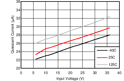
VFB = 1.2 V
Figure 7-1 Non-Switching Input Supply Current
GUID-05DD648F-94E0-4C17-8411-29B9BF9BDF0B-low.png
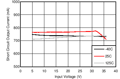
VOUT = 0 VƒS = 400 kHzSee Figure 9-27
Figure 7-3 Short-Circuit Output Current
GUID-8C2AC3D2-F871-4A6F-9DA2-B0770CB29ACC-low.gif
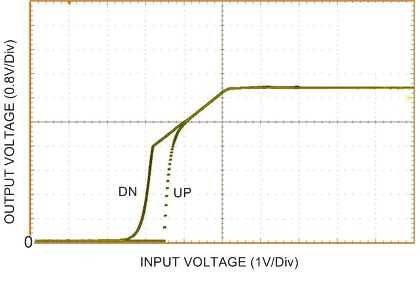
IOUT = 1 mASee Figure 9-27
Figure 7-5 UVLO Thresholds
GUID-ACEDAAB2-A3D7-4B27-93FB-06A5DFE1AACD-low.png
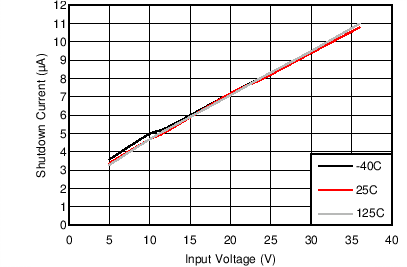
EN = 0 V
Figure 7-2 Shutdown Supply Current
GUID-A1749306-C32A-4441-865A-F654BDF1DD15-low.png
 
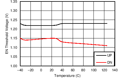
Figure 7-4 Precision Enable Thresholds
GUID-094A10BB-151A-4FCB-9BF2-F154B2DC012F-low.png
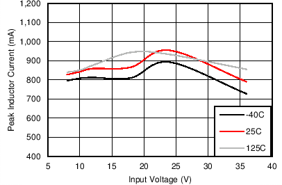
IOUT = 0 AVOUT = 5 VSee Figure 9-27
ƒSW = 400 kHz
Figure 7-6 IPEAK-MIN