SNVSBQ5 June 2021 LMR33620AP-Q1 , LMR33630AP-Q1
PRODUCTION DATA
- 1 Features
- 2 Applications
- 3 Description
- 4 Revision History
- 5 Device Comparison Table
- 6 Pin Configuration and Functions
- 7 Specifications
- 8 Detailed Description
-
9 Application and Implementation
- 9.1 Application Information
- 9.2
Typical Application
- 9.2.1 Design Requirements
- 9.2.2
Detailed Design Procedure
- 9.2.2.1 Custom Design With WEBENCH® Tools
- 9.2.2.2 Choosing the Switching Frequency
- 9.2.2.3 Setting the Output Voltage
- 9.2.2.4 Inductor Selection
- 9.2.2.5 Output Capacitor Selection
- 9.2.2.6 Input Capacitor Selection
- 9.2.2.7 CBOOT
- 9.2.2.8 VCC
- 9.2.2.9 CFF Selection
- 9.2.2.10 External UVLO
- 9.2.2.11 Maximum Ambient Temperature
- 9.2.3 Application Curves
- 9.3 What to Do and What Not to Do
- 10Power Supply Recommendations
- 11Layout
- 12Device and Documentation Support
- 13Mechanical, Packaging, and Orderable Information
Package Options
Mechanical Data (Package|Pins)
- RNX|12
Thermal pad, mechanical data (Package|Pins)
- RNX|12
Orderable Information
9.2.2.3 Setting the Output Voltage
The output voltage of the LMR336x0AP-Q1 is externally adjustable using a resistor divider network. The range of recommended output voltage is found in Section 7.3. The divider network is comprised of RFBT and RFBB, and closes the loop between the output voltage and the converter. The converter regulates the output voltage by holding the voltage on the FB pin equal to the internal reference voltage, VREF. The resistance of the divider is a compromise between excessive noise pickup and excessive loading of the output. Smaller values of resistance reduce noise sensitivity but also reduce the light-load efficiency. The recommended value for RFBT is 100 kΩ; with a maximum value of 1 MΩ. If a 1 MΩ is selected for RFBT, then a feedforward capacitor must be used across this resistor to provide adequate loop phase margin (see Section 9.2.2.9). Once RFBT is selected, Equation 3 is used to select RFBB. VREF is nominally 1 V (see Section 7.5 for limits).
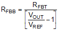
For this 5-V example, RFBT = 100 kΩ and RFBB = 24.9 kΩ are chosen.