SNVSAY7D August 2018 – August 2022 LMR36006-Q1
PRODUCTION DATA
- 1 Features
- 2 Applications
- 3 Description
- 4 Revision History
- 5 Device Comparison Table
- 6 Pin Configuration and Functions
- 7 Specifications
- 8 Detailed Description
-
9 Application and Implementation
- 9.1 Application Information
- 9.2
Typical Application
- 9.2.1
Design 1: Low Power 24-V, 600-mA PFM Converter
- 9.2.1.1 Design Requirements
- 9.2.1.2
Detailed Design Procedure
- 9.2.1.2.1 Custom Design With WEBENCH Tools
- 9.2.1.2.2 Choosing the Switching Frequency
- 9.2.1.2.3 Setting the Output Voltage
- 9.2.1.2.4 Inductor Selection
- 9.2.1.2.5 Output Capacitor Selection
- 9.2.1.2.6 Input Capacitor Selection
- 9.2.1.2.7 CBOOT
- 9.2.1.2.8 VCC
- 9.2.1.2.9 CFF Selection
- 9.2.1.2.10 Maximum Ambient Temperature
- 9.2.1.3 Application Curves
- 9.2.2 Design 2: High Density 12-V , 600-mA FPWM Converter
- 9.2.1
Design 1: Low Power 24-V, 600-mA PFM Converter
- 9.3 What to Do and What Not to Do
- 10Power Supply Recommendations
- 11Layout
- 12Device and Documentation Support
- 13Mechanical, Packaging, and Orderable Information
Package Options
Mechanical Data (Package|Pins)
- RNX|12
Thermal pad, mechanical data (Package|Pins)
- RNX|12
Orderable Information
3 Description
The LMR36006-Q1 regulator is an easy-to-use, synchronous, step-down DC/DC converter. With integrated high-side and low-side power MOSFETs, up to 0.6 A of output current is delivered over a wide input voltage range of 4.2 V to 60 V. Tolerance goes up to 66 V.
The LMR36006-Q1 uses peak-current-mode control to provide optimal efficiency and output voltage accuracy. Advanced high speed circuitry allows the LMR36006-Q1 to regulate from an input of 20 V to an output of 5 V at a fixed frequency of 2.1 MHz. Precision enable gives flexibility by enabling a direct connection to the wide input voltage or precise control over device start-up and shutdown. The power-good flag, with built-in filtering and delay, offers a true indication of system status eliminating the requirement for an external supervisor.
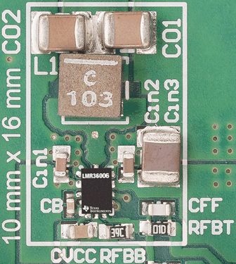
The LMR36006-Q1 is in a HotRod™ package which enables low EMI, higher efficiency, and the smallest package to die ratio. The device requires few external components and has a pinout designed for simple PCB layout. The small solution size and feature set of the LMR36006-Q1 are designed to simplify implementation for a wide range of end equipment.
| PART NUMBER | PACKAGE(1) | BODY SIZE (NOM) |
|---|---|---|
| LMR36006-Q1 | VQFN-HR (12) | 2.00 mm × 3.00 mm |

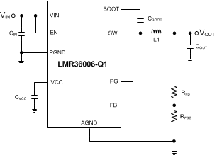
 Simplified Schematic