SNVSAY7D August 2018 – August 2022 LMR36006-Q1
PRODUCTION DATA
- 1 Features
- 2 Applications
- 3 Description
- 4 Revision History
- 5 Device Comparison Table
- 6 Pin Configuration and Functions
- 7 Specifications
- 8 Detailed Description
-
9 Application and Implementation
- 9.1 Application Information
- 9.2
Typical Application
- 9.2.1
Design 1: Low Power 24-V, 600-mA PFM Converter
- 9.2.1.1 Design Requirements
- 9.2.1.2
Detailed Design Procedure
- 9.2.1.2.1 Custom Design With WEBENCH Tools
- 9.2.1.2.2 Choosing the Switching Frequency
- 9.2.1.2.3 Setting the Output Voltage
- 9.2.1.2.4 Inductor Selection
- 9.2.1.2.5 Output Capacitor Selection
- 9.2.1.2.6 Input Capacitor Selection
- 9.2.1.2.7 CBOOT
- 9.2.1.2.8 VCC
- 9.2.1.2.9 CFF Selection
- 9.2.1.2.10 Maximum Ambient Temperature
- 9.2.1.3 Application Curves
- 9.2.2 Design 2: High Density 12-V , 600-mA FPWM Converter
- 9.2.1
Design 1: Low Power 24-V, 600-mA PFM Converter
- 9.3 What to Do and What Not to Do
- 10Power Supply Recommendations
- 11Layout
- 12Device and Documentation Support
- 13Mechanical, Packaging, and Orderable Information
Package Options
Mechanical Data (Package|Pins)
- RNX|12
Thermal pad, mechanical data (Package|Pins)
- RNX|12
Orderable Information
9.2.1.2.9.1 External UVLO
In some cases, an input UVLO level different than that provided internal to the device is needed. This can be accomplished by using the circuit shown in Figure 9-3 can be used. The input voltage at which the device turns on is designated VON; while the turnoff voltage is VOFF. First, a value for RENB is chosen in the range of 10 kΩ to 100 kΩ and then Equation 10 is used to calculate RENT and VOFF.
 Figure 9-3 Setup for External UVLO
Application
Figure 9-3 Setup for External UVLO
ApplicationEquation 10. 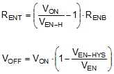
where
- VON = VIN turnon voltage
- VOFF = VIN turnoff voltage