SNVSAY7D August 2018 – August 2022 LMR36006-Q1
PRODUCTION DATA
- 1 Features
- 2 Applications
- 3 Description
- 4 Revision History
- 5 Device Comparison Table
- 6 Pin Configuration and Functions
- 7 Specifications
- 8 Detailed Description
-
9 Application and Implementation
- 9.1 Application Information
- 9.2
Typical Application
- 9.2.1
Design 1: Low Power 24-V, 600-mA PFM Converter
- 9.2.1.1 Design Requirements
- 9.2.1.2
Detailed Design Procedure
- 9.2.1.2.1 Custom Design With WEBENCH Tools
- 9.2.1.2.2 Choosing the Switching Frequency
- 9.2.1.2.3 Setting the Output Voltage
- 9.2.1.2.4 Inductor Selection
- 9.2.1.2.5 Output Capacitor Selection
- 9.2.1.2.6 Input Capacitor Selection
- 9.2.1.2.7 CBOOT
- 9.2.1.2.8 VCC
- 9.2.1.2.9 CFF Selection
- 9.2.1.2.10 Maximum Ambient Temperature
- 9.2.1.3 Application Curves
- 9.2.2 Design 2: High Density 12-V , 600-mA FPWM Converter
- 9.2.1
Design 1: Low Power 24-V, 600-mA PFM Converter
- 9.3 What to Do and What Not to Do
- 10Power Supply Recommendations
- 11Layout
- 12Device and Documentation Support
- 13Mechanical, Packaging, and Orderable Information
Package Options
Mechanical Data (Package|Pins)
- RNX|12
Thermal pad, mechanical data (Package|Pins)
- RNX|12
Orderable Information
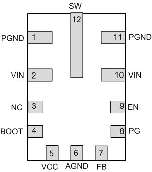
6 Pin Configuration and Functions
 Figure 6-1 12-Pin VQFN-HR RNX Package (Top View)
Table 6-1 Pin Functions
| NO. | NAME | TYPE | DESCRIPTION |
|---|---|---|---|
| 1, 11 | PGND | G | Power ground terminal. Connect to system ground and AGND. Connect to CIN with short wide traces. |
| 2, 10 | VIN | P | Input supply to regulator. Connect to CIN with short wide traces. |
| 3 | NC | — | Connect the SW pin to NC on the PCB. This simplifies the connection from the CBOOT capacitor to the SW pin. This pin has no internal connection to the regulator. |
| 4 | BOOT | P | Bootstrap supply voltage for internal high-side driver. Connect a high-quality 100-nF capacitor from this pin to the SW pin. Connect the SW pin to NC on the PCB. This simplifies the connection from the CBOOT capacitor to the SW pin. |
| 5 | VCC | P | Internal 5-V LDO output. Used as supply to internal control circuits. Do not connect to external loads. Can be used as logic supply for power-good flag. Connect a high-quality 1-µF capacitor from this pin to GND. |
| 6 | AGND | G | Analog ground for regulator and system. Ground reference for internal references and logic. All electrical parameters are measured with respect to this pin. Connect to system ground on PCB. |
| 7 | FB | A | Feedback input to regulator. Connect to output voltage node for fixed VOUT applications. Connect to tap point of feedback voltage divider. Do not float. Do not ground. |
| 8 | PG | A | Open-drain power-good flag output. Connect to suitable voltage supply through a current limiting resistor. High = power OK, low = power bad. Goes low when EN = Low. Can be open or grounded when not used. |
| 9 | EN | A | Enable input to regulator. High = ON, low = OFF. Can be connected directly to VIN; Do not float. |
| 12 | SW | P | Regulator switch node. Connect to power inductor. Connect the SW pin to NC on the PCB. This simplifies the connection from the CBOOT capacitor to the SW pin. |
| A = Analog, P = Power, G = Ground | |||