SLOS263Y august 1999 – august 2023 LMV321 , LMV324 , LMV358
PRODUCTION DATA
- 1
- 1 Features
- 2 Applications
- 3 Description
- 4 Revision History
- 5 Pin Configuration and Functions
- 6 Specifications
- 7 Detailed Description
- 8 Application and Implementation
- 9 Device and Documentation Support
- 10Mechanical, Packaging, and Orderable Information
Package Options
Refer to the PDF data sheet for device specific package drawings
Mechanical Data (Package|Pins)
- D|8
- DGK|8
- PW|8
Thermal pad, mechanical data (Package|Pins)
Orderable Information
8.1.3 Application Curves
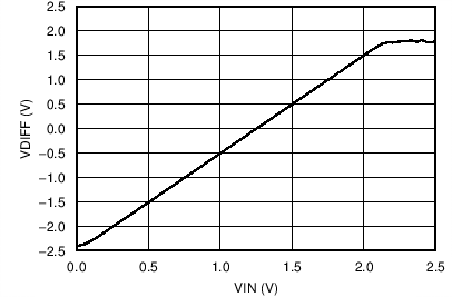
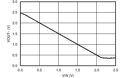
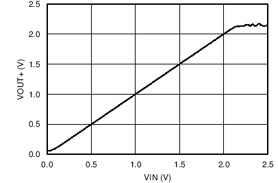
The measured transfer functions in Figure 8-2, Figure 8-3, and Figure 8-4 were generated by sweeping the input voltage from 0 V to 2.5 V. However, this design should only be used between 0.5 V and 2 V for optimum linearity.
 Figure 8-2 Differential Output Voltage vs Input Voltage
 Figure 8-4 Positive Output Voltage Node vs Input Voltage
 Figure 8-3 Positive Output Voltage Node vs Input Voltage