SNOSD09 September 2015 LMV7275-Q1
PRODUCTION DATA.
- 1 Features
- 2 Applications
- 3 Description
- 4 Revision History
- 5 Pin Configuration and Functions
-
6 Specifications
- 6.1 Absolute Maximum Ratings
- 6.2 ESD Ratings LMV7275-Q1
- 6.3 Recommended Operating Conditions
- 6.4 Thermal Information
- 6.5 1.8-V Electrical Characteristics
- 6.6 1.8-V AC Electrical Characteristics
- 6.7 2.7-V Electrical Characteristics
- 6.8 2.7-V AC Electrical Characteristics
- 6.9 5-V Electrical Characteristics
- 6.10 5-V AC Electrical Characteristics
- 6.11 Typical Characteristics
- 7 Detailed Description
- 8 Application and Implementation
- 9 Power Supply Recommendations
- 10Layout
- 11Device and Documentation Support
- 12Mechanical, Packaging, and Orderable Information
Package Options
Mechanical Data (Package|Pins)
- DCK|5
Thermal pad, mechanical data (Package|Pins)
Orderable Information
7 Detailed Description
7.1 Overview
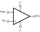
A comparator is often used to convert an analog signal to a digital signal. As shown in Figure 18, the comparator compares an input voltage (VIN) to a reference voltage (VREF). If VIN is less than VREF, the output transistor turns on and pulls the output to V-, and thus the output (VO) goes low.
However, if VIN is greater than VREF, the output transistor turns off and the voltage (VO) is pulled high by the external pull-up resistor.
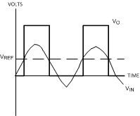 Figure 18. Basic Comparator
7.2 Functional Block Diagram
7.3 Feature Description
7.3.1 Rail-to-Rail Input Stage
The LMV7275-Q1 has an input common mode voltage range (VCM) of −0.1V below the V− to 0.1 V above V+. This is achieved by using paralleled PNP and NPN differential input pairs. When the VCM is near V+, the NPN pair is on and the PNP pair is off. When the VCM is near V−, the NPN pair is off and the PNP pair is on. The crossover point between the NPN and PNP input stages is around 950mV from V+. Because each input stage has its own offset voltage (VOS), the VOS of the comparator becomes a function of the VCM. See curves for VOS vs. VCM in the Typical Characteristics section. In application design, it is recommended to keep the VCM away from the crossover point to avoid problems. The wide input voltage range makes LMV7275-Q1 ideal in power supply monitoring circuits, where the comparators are used to sense signals close to ground and power supplies.
7.3.2 Output Stage
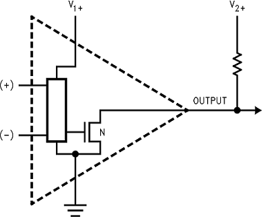 Figure 19. LMV7275-Q1 Open-Drain Output
The LMV7275-Q1 has an open-drain output that requires a pull-up resistor to a positive supply voltage for the output to operate properly. When the internal output transistor is off, the output voltage will be pulled up to the external positive voltage (V2+) by the external pull-up resistor. This allows the output to be OR'ed with other open-drain outputs on the same bus.
The output pull-up resistor may be connected to any voltage level between V- and V+ for level shifting applications.
7.4 Device Functional Modes
7.4.1 Capacitive and Resistive Loads
The propagation delay on the rising edge of the LMV7275-Q1 depends on the load resistance and capacitance values.
7.4.2 Noise
Most comparators have rather low gain. This allows the output to alternate between high and low when the input signal changes slowly. The result is the output may oscillate between high and low when the differential input is near zero and triggers on noise. The high gain of this comparator eliminates this problem. Less than 1 μV of change on the input will drive the output from one rail to the other rail. If the input signal is noisy, the output cannot ignore the noise unless some hysteresis is provided by positive feedback. (See Hysteresis.)
7.4.3 Hysteresis
It is a standard procedure to use hysteresis (positive feedback) around a comparator to prevent oscillation due to the comparator triggering its own noise on slowly ramping signals. The following sections will describe various ways to apply hysteresis.
7.4.3.1 Non-inverting Comparator With Hysteresis
Non-inverting comparator with hysteresis requires a two resistor network, and a voltage reference (Vref) at the inverting input. When Vin is low, the output is also low. For the output to switch from low to high, Vin must rise up to Vin1 where Vin1 is calculated by:

When Vin is high, the output is also high. To make the comparator switch back to its low state, Vin must equal Vref before VA will again equal Vref. Vin can be calculated by:

The hysteresis of this circuit is the difference between Vin1 and Vin2.
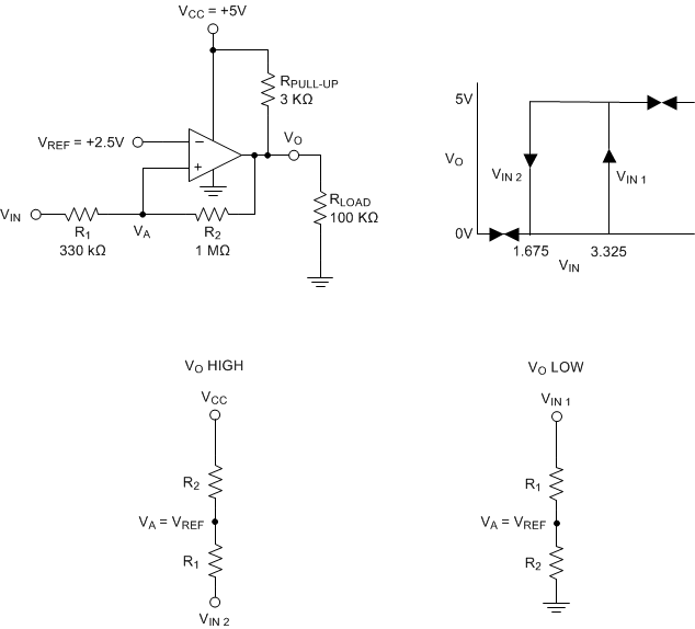 Figure 20. Non-Inverting Comparator With Hysteresis
7.4.3.2 Inverting Comparator With Hysteresis
The inverting comparator with hysteresis requires a three resistor network that are referenced to the supply voltage VCC of the comparator. When Vin at the inverting input is less than Va, the voltage at the non-inverting node of the comparator (Vin < Va), the output voltage is high (for simplicity assume VO switches as high as VCC). The three network resistors can be represented as R1//R3 in series with R2. The lower input trip voltage Va1 is defined as:

When Vin is greater than Va (Vin > Va), the output voltage is low very close to ground. In this case the three network resistors can be presented as R2//R3 in series with R1. The upper trip voltage Va2 is defined as:

The total hysteresis provided by the network is defined as:
To assure that the comparator will always switch fully to VCC and not be pulled down by the load the resistors values should be chosen as follow:
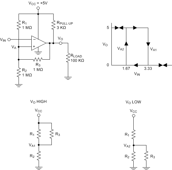 Figure 21. Inverting Comparator With Hysteresis
7.4.4 Zero Crossing Detector
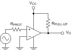 Figure 22. Simple Zero Crossing Detector
In a zero crossing detector circuit, the inverting input is connected to ground and the Non-Inverting input is connected to a 100 mVPP AC signal. As the signal at the Non-Inverting input crosses 0 V, the output of the comparator changes state.
RPROT is an optional input protection resistor to limit the current should the input voltage exceed the supply rails. RPROT should be a minimum of 1 kΩ per volt of expected over-voltage and limit the current to less than ±1mA under worst case fault conditions.
7.4.4.1 Zero Crossing Detector With Hysteresis
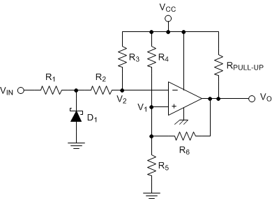 Figure 23. Zero Crossing Detector With Hysteresis
To improve switching times and centering the input threshold to ground a small amount of positive feedback is added to the circuit. Voltage divider R4 and R5 establishes a reference voltage, V1, at the positive input. By making the series resistance, R1 plus R2 equal to R5, the switching condition, V1 = V2, will be satisfied when VIN = 0.
The positive feedback resistor, R6, is made very large (with respect to R5 || R6 = 2000 R5). The resultant hysteresis established by this network is very small (ΔV1 < 10 mV) but it is sufficient to insure rapid output voltage transitions.
Diode D1 is used to insure that the inverting input terminal of the comparator never goes below approximately −100 mV. As the input terminal goes negative, D1 will forward bias, clamping the node between R1 and R2 to approximately −300 mV. This sets up a voltage divider with R2 and R3 preventing V2 from going below ground. The maximum negative input overdrive is limited by the current handling ability of D1.
7.4.5 Threshold Detector
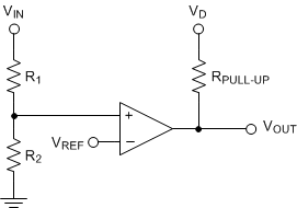 Figure 24. Threshold Detector
Instead of tying the inverting input to 0 V, the inverting input can be tied to a reference voltage. As the input on the Non-Inverting input passes the VREF threshold, the output of the comparator changes state. It is important to use a stable reference voltage to ensure a consistent switching point.
7.4.6 Universal Logic Level Shifter
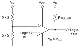 Figure 25. Logic Level Shifter
The output of LMV7275-Q1 is an unconnected drain of an NMOS device, which can be pulled up, through a resistor, to any desired output level below the comparators power supply voltage (VB ≤ VCC). Hence, the following simple circuit works as a universal logic level shifter, pulling up the signal to the desired level.
For example, VA could be the 5-V analog supply voltage, where VB could be the 3.3-V supply of the processor. The output will now be compatible with the 3.3-V logic.
7.4.7 OR'ING the Output
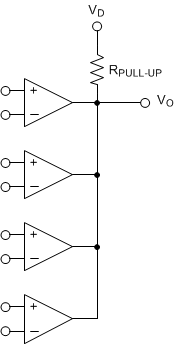 Figure 26. OR’ing the Outputs
Open-drain outputs may be tied together, pulled up to VD by a common resistor to provide an output OR'ing function. If any of the comparator outputs goes low, the output VO goes low.