SNOSD09 September 2015 LMV7275-Q1
PRODUCTION DATA.
- 1 Features
- 2 Applications
- 3 Description
- 4 Revision History
- 5 Pin Configuration and Functions
-
6 Specifications
- 6.1 Absolute Maximum Ratings
- 6.2 ESD Ratings LMV7275-Q1
- 6.3 Recommended Operating Conditions
- 6.4 Thermal Information
- 6.5 1.8-V Electrical Characteristics
- 6.6 1.8-V AC Electrical Characteristics
- 6.7 2.7-V Electrical Characteristics
- 6.8 2.7-V AC Electrical Characteristics
- 6.9 5-V Electrical Characteristics
- 6.10 5-V AC Electrical Characteristics
- 6.11 Typical Characteristics
- 7 Detailed Description
- 8 Application and Implementation
- 9 Power Supply Recommendations
- 10Layout
- 11Device and Documentation Support
- 12Mechanical, Packaging, and Orderable Information
Package Options
Mechanical Data (Package|Pins)
- DCK|5
Thermal pad, mechanical data (Package|Pins)
Orderable Information
6 Specifications
6.1 Absolute Maximum Ratings (1)
| MIN | MAX | UNIT | ||
|---|---|---|---|---|
| VIN Differential | ±Supply Voltage | V | ||
| Supply Voltage (V+ - V−) | 6 | V | ||
| Voltage at Input/Output pins | (V−) − 0.1 | (V+) + 0.1 | V | |
| Junction Temperature(2) | 150 | °C | ||
| Storage Temperature, Tstg | –65 | 150 | °C | |
(1) Stresses beyond those listed under Absolute Maximum Ratings may cause permanent damage to the device. These are stress ratings only, which do not imply functional operation of the device at these or any other conditions beyond those indicated under Recommended Operating Conditions. Exposure to absolute-maximum-rated conditions for extended periods may affect device reliability.
(2) The maximum power dissipation is a function of TJ(MAX), RθJA, and TA. The maximum allowable power dissipation at any ambient temperature is PD = (TJ(MAX) - TA)/RθJA. All numbers apply for packages soldered directly into a PCB.
6.2 ESD Ratings LMV7275-Q1
| VALUE | UNIT | |||
|---|---|---|---|---|
| V(ESD) | Electrostatic discharge | Human-body model (HBM), per AEC Q100-002(1) | ±2000 | V |
| Charged-device model (CDM), per AEC Q100-011 | ±1000 | |||
(1) AEC Q100-002 indicates that HBM stressing shall be in accordance with the ANSI/ESDA/JEDEC JS-001 specification.
6.3 Recommended Operating Conditions
| MIN | MAX | UNIT | |
|---|---|---|---|
| Supply Voltage | 1.8 | 5.5 | V |
| Temperature(1) | –40 | 85 | °C |
(1) The maximum power dissipation is a function of TJ(MAX), RθJA, and TA. The maximum allowable power dissipation at any ambient temperature is PD = (TJ(MAX) - TA)/RθJA. All numbers apply for packages soldered directly into a PCB.
6.4 Thermal Information
| THERMAL METRIC(1) | LMV7275-Q1 | UNIT | |
|---|---|---|---|
| DGK (SC70) | |||
| 5 PINS | |||
| RθJA | Junction-to-ambient thermal resistance (2) | 273.8 | °C/W |
| RθJC(top) | Junction-to-case (top) thermal resistance | 106.1 | °C/W |
| RθJB | Junction-to-board thermal resistance | 54.9 | °C/W |
| ψJT | Junction-to-top characterization parameter | 3.6 | °C/W |
| ψJB | Junction-to-board characterization parameter | 54.1 | °C/W |
(1) For more information about traditional and new thermal metrics, see the Semiconductor and IC Package Thermal Metrics application report, SPRA953.
(2) The maximum power dissipation is a function of TJ(MAX), RθJA, and TA. The maximum allowable power dissipation at any ambient temperature is PD = (TJ(MAX) - TA)/RθJA. All numbers apply for packages soldered directly into a PCB.
6.5 1.8-V Electrical Characteristics
Unless otherwise specified, all limits ensured for TJ = 25°C, V+ = 1.8 V, V− = 0 V.| PARAMETER | CONDITION | MIN(2) | TYP(1) | MAX(2) | UNIT | ||
|---|---|---|---|---|---|---|---|
| VOS | Input Offset Voltage | 0.3 | 4 | mV | |||
| At the temperature extremes | 6 | ||||||
| TC VOS | Input Offset Temperature Drift | VCM = 0.9 V (3) | 20 | uV/°C | |||
| IB | Input Bias Current | 10 | nA | ||||
| IOS | Input Offset Current | 200 | pA | ||||
| IS | Supply Current | 9 | 12 | µA | |||
| At the temperature extremes | 14 | ||||||
| ISC | Output Short Circuit Current | Sinking, VO = 0.9 V | 4 | 6 | mA | ||
| VOL | Output Voltage Low | IO = −0.5 mA | 52 | 100 | mV | ||
| IO = −1.5 mA | 166 | 220 | |||||
| VCM | Input Common-Mode Voltage Range | CMRR > 45 dB | −0.1 | 1.9 | V | ||
| CMRR | Common-Mode Rejection Ratio | 0 < VCM < 1.8 V | 46 | 78 | dB | ||
| PSRR | Power Supply Rejection Ratio | V+ = 1.8 V to 5 V | 55 | 80 | dB | ||
| ILEAKAGE | Output Leakage Current | VO = 1.8 V | 2 | pA | |||
(1) Typical values represent the most likely parametric norm.
(2) All limits are ensured by testing or statistical analysis.
(3) Offset Voltage average drift determined by dividing the change in VOS at temperature extremes into the total temperature change.
6.6 1.8-V AC Electrical Characteristics
Unless otherwise specified, all limits ensured for TJ = 25°C, V+ = 1.8 V, V− = 0 V, VCM = 0.5 V, VO = V+/2 and RL > 1 MΩ to V−.| PARAMETER | CONDITION | MIN(2) | TYP(1) | MAX(2) | UNIT | |
|---|---|---|---|---|---|---|
| tPHL | Propagation Delay (High to Low) |
Input Overdrive = 20 mV Load = 50 pF//5 kΩ |
880 | ns | ||
| Input Overdrive = 50 mV Load = 50 pF//5 kΩ |
570 | ns | ||||
| tPLH | Propagation Delay (Low to High) |
Input Overdrive = 20 mV Load = 50 pF//5 kΩ |
1100 | ns | ||
| Input Overdrive = 50 mV Load = 50 pF//5 kΩ |
800 | ns | ||||
6.7 2.7-V Electrical Characteristics
Unless otherwise specified, all limits ensured for TJ = 25°C, V+ = 2.7 V, V− = 0 V.| PARAMETER | CONDITIONS | MIN(2) | TYP(1) | MAX(2) | UNIT | ||
|---|---|---|---|---|---|---|---|
| VOS | Input Offset Voltage | 0.3 | 4 | mV | |||
| At the temperature extremes | 6 | ||||||
| TC VOS | Input Offset Temperature Drift | VCM = 1.35 V(3) | 20 | µV/°C | |||
| IB | Input Bias Current | 10 | nA | ||||
| IOS | Input offset Current | 200 | pA | ||||
| IS | Supply Current | 9 | 13 | µA | |||
| At the temperature extremes | 15 | ||||||
| ISC | Output Short Circuit Current | Sinking, VO = 1.35 V | 10 | 15 | mA | ||
| VOL | Output Voltage Low | IO = −0.5 mA | 50 | 70 | mV | ||
| IO = −2 mA | 155 | 220 | |||||
| VCM | Input Common Voltage Range | CMRR > 45 dB | −0.1 | 2.8 | V | ||
| CMRR | Common-Mode Rejection Ratio | 0 < VCM < 2.7 V | 46 | 78 | dB | ||
| PSRR | Power Supply Rejection Ratio | V+ = 1.8 V to 5 V | 55 | 80 | dB | ||
| ILEAKAGE | Output Leakage Current | VO = 2.7 V | 2 | pA | |||
6.8 2.7-V AC Electrical Characteristics
Unless otherwise specified, all limits ensured for TJ = 25°C, V+ = 2.7 V, V− = 0 V, VCM = 0.5 V, VO = V+/2 and RL > 1 MΩ to V−.| PARAMETER | CONDITION | MIN(2) | TYP(1) | MAX(2) | UNIT | |
|---|---|---|---|---|---|---|
| tPHL | Propagation Delay (High to Low) |
Input Overdrive = 20 mV Load = 50 pF//5 kΩ |
1200 | ns | ||
| Input Overdrive = 50 mV Load = 50 pF//5 kΩ |
810 | ns | ||||
| tPLH | Propagation Delay (Low to High) |
Input Overdrive = 20 mV Load = 50 pF//5 kΩ |
1300 | ns | ||
| Input Overdrive = 50 mV Load = 50 pF//5 kΩ |
860 | ns | ||||
6.9 5-V Electrical Characteristics
Unless otherwise specified, all limits ensured for TJ = 25°C, V+ = 5 V, V− = 0 V.| PARAMETER | CONDITIONS | MIN(2) | TYP(1) | MAX(2) | UNIT | ||
|---|---|---|---|---|---|---|---|
| VOS | Input Offset Voltage | 0.3 | 4 | mV | |||
| At the temperature extremes | 6 | ||||||
| TC VOS | Input Offset Temperature Drift | VCM = 2.5 V(3) | 20 | µV/°C | |||
| IB | Input Bias Current | 10 | nA | ||||
| IOS | Input Offset Current | 200 | pA | ||||
| IS | Supply Current | 10 | 14 | µA | |||
| 16 | |||||||
| At the temperature extremes | |||||||
| ISC | Output Short Circuit Current | Sinking, VO = 2.5 V | 18 | 34 | mA | ||
| VOL | Output Voltage Low | IO = −0.5 mA | 27 | 70 | mV | ||
| IO = −4.0 mA | 225 | 315 | |||||
| VCM | Input Common Voltage Range | CMRR > 45 dB | −0.1 | 5.1 | V | ||
| CMRR | Common-Mode Rejection Ratio | 0 < VCM < 5.0 V | 46 | 78 | dB | ||
| PSRR | Power Supply Rejection Ratio | V+ = 1.8 V to 5 V | 55 | 80 | dB | ||
| ILEAKAGE | Output Leakage Current | VO = 5 V | 2 | pA | |||
6.10 5-V AC Electrical Characteristics
Unless otherwise specified, all limits ensured for TJ = 25°C, V+ = 5.0 V, V− = 0 V, VCM = 0.5 V, VO = V+/2 and RL > 1 MΩ to V−.| PARAMETER | CONDITION | MIN(2) | TYP(1) | MAX(2) | UNIT | |
|---|---|---|---|---|---|---|
| tPHL | Propagation Delay (High to Low) |
Input Overdrive = 20 mV Load = 50 pF//5 kΩ |
2100 | ns | ||
| Input Overdrive = 50 mV Load = 50 pF//5 kΩ |
1380 | ns | ||||
| tPLH | Propagation Delay (Low to High) |
Input Overdrive = 20 mV Load = 50 pF//5 kΩ |
1800 | ns | ||
| Input Overdrive = 50 mV Load = 50 pF//5 kΩ |
1100 | ns | ||||
6.11 Typical Characteristics
TA = 25°C, Unless otherwise specified.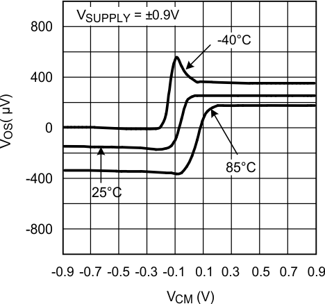 Figure 1. VOS vs. VCM
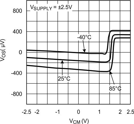 Figure 3. VOS vs. VCM
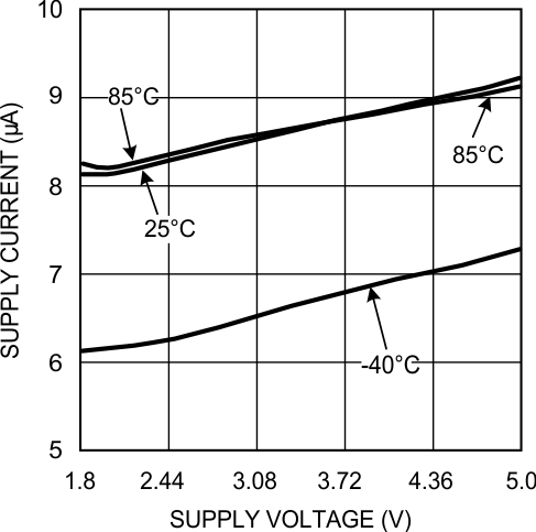 Figure 5. Supply Current vs. Supply Voltage
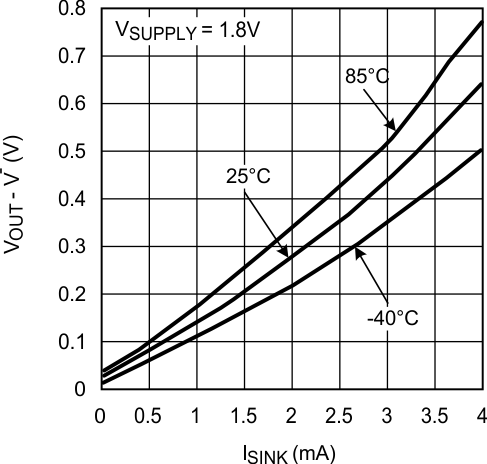 Figure 7. Output Negative Swing vs. ISINK
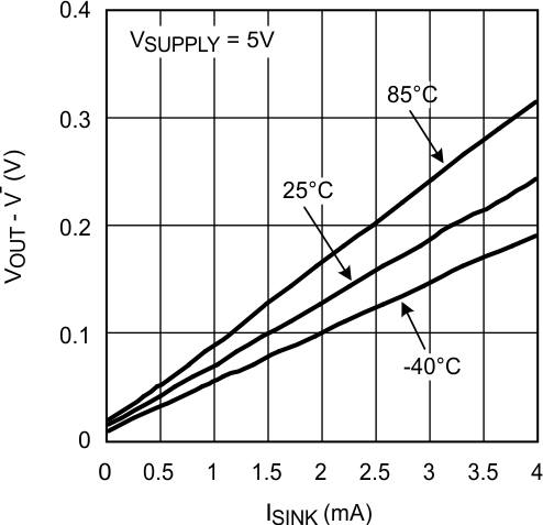 Figure 9. Output Negative Swing vs. ISINK
 Figure 11. Propagation Delay (tPHL)
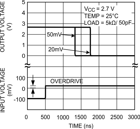 Figure 13. Propagation Delay (tPHL)
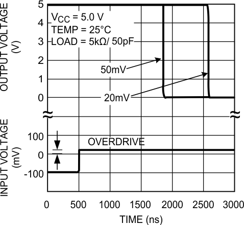 Figure 15. Propagation Delay (tPHL)
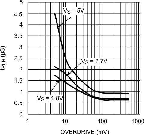 Figure 17. tPLH vs. Overdrive
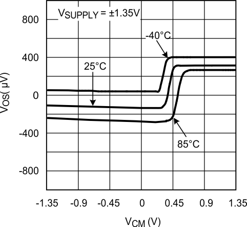 Figure 2. VOS vs. VCM
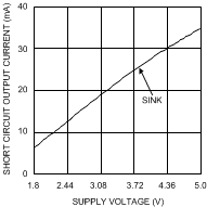 Figure 4. Short Circuit vs. Supply Voltage
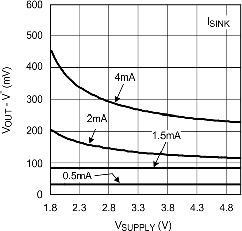 Figure 6. Output Negative Swing vs. VSUPPLY
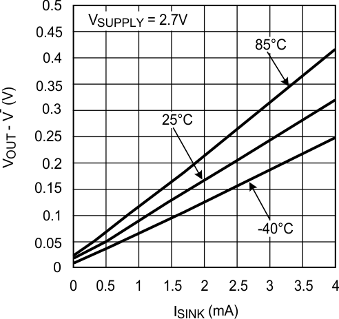 Figure 8. Output Negative Swing vs. ISINK
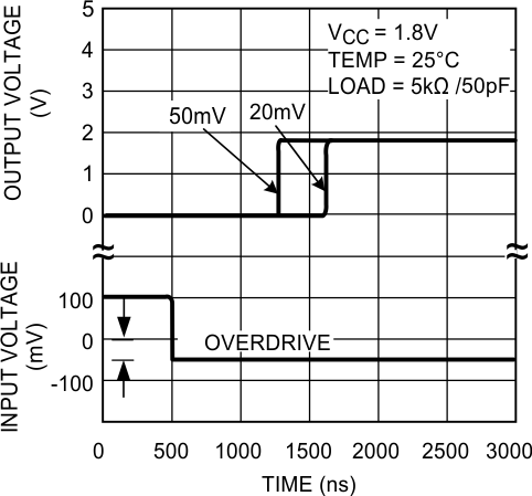 Figure 10. Propagation Delay (tPLH)
 Figure 12. Propagation Delay (tPLH)
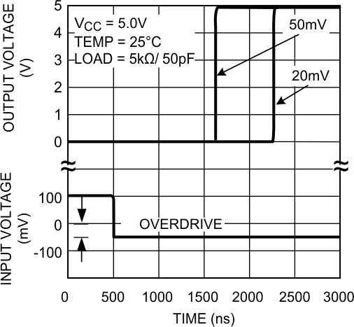 Figure 14. Propagation Delay (tPLH)
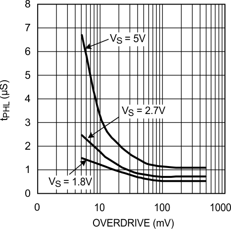 Figure 16. tPHL vs. Overdrive