SNOSAG6G September 2005 – October 2015 LMV791 , LMV792
PRODUCTION DATA.
- 1 Features
- 2 Applications
- 3 Description
- 4 Revision History
- 5 Pin Configuration and Functions
- 6 Specifications
- 7 Detailed Description
- 8 Application and Implementation
- 9 Power Supply Recommendations
- 10Layout
- 11Device and Documentation Support
- 12Mechanical, Packaging, and Orderable Information
Package Options
Mechanical Data (Package|Pins)
- DGS|10
Thermal pad, mechanical data (Package|Pins)
Orderable Information
7 Detailed Description
7.1 Overview
The LMV79x family provides optimal performance in low-voltage and low-noise systems. A low-noise CMOS input stage, with typical input bias currents in the range of a few femtoamperes, and an input common-mode voltage range which includes ground make the LMV791 and the LMV792 ideal for low-power sensor applications
7.2 Functional Block Diagram
7.3 Feature Description
7.3.1 Wide Bandwidth at Low Supply Current
The LMV791 and LMV792 are high performance operational amplifiers that provide a unity gain bandwidth of 17 MHz while drawing a low supply current of 1.15 mA. This makes them ideal for providing wideband amplification in portable applications. The shutdown feature can also be used to design more power efficient systems that offer wide bandwidth and high performance while consuming less average power.
7.3.2 Low Input Referred Noise and Low Input Bias Current
The LMV79x have a very low input referred voltage noise density (5.8 nV/√Hz at 1 kHz). A CMOS input stage ensures a small input bias current (100 fA) and low input referred current noise (0.01 pA/√Hz). This is very helpful in maintaining signal fidelity, and makes the LMV791 and LMV792 ideal for audio and sensor-based applications.
7.3.3 Low Supply Voltage
The LMV791 and the LMV792 have performance ensured at 2.5-V and 5-V supply. The LMV791 family is ensured to be operational at all supply voltages between 2 V and 5.5 V, for ambient temperatures ranging from −40°C to 125°C, thus using the entire battery lifetime. The LMV791 and LMV792 are also ensured to be operational at 1.8-V supply voltage, for temperatures between 0°C and 125°C. This makes the LMV791 family ideal for usage in low-voltage commercial applications.
7.3.4 Rail-to-Rail Output and Ground Sensing
Rail-to-rail output swing provides maximum possible dynamic range at the output. This is particularly important when operating at low supply voltages. An innovative positive feedback scheme is used to boost the current drive capability of the output stage. This allows the LMV791 and the LMV792 to source more than 40 mA of current at 1.8-V supply. This also limits the performance of the LMV791 family as comparators, and hence the usage of the LMV791 and the LMV792 in an open-loop configuration is not recommended. The input common-mode range includes the negative supply rail which allows direct sensing at ground in single supply operation.
7.3.5 Shutdown Feature
The LMV791 family is ideal for battery-powered systems. With a low supply current of 1.15 mA and a shutdown current of 140 nA typically, the LMV791 and LMV792 allow the designer to maximize battery life. The enable pin of the LMV791 and the LMV792 allows the operational amplifier to be turned off and reduce its supply current to less than 1 μA. To power on the operational amplifier the enable pin should be higher than V+ – 0.5 V, where V+ is the positive supply. To disable the operational amplifier, the enable pin voltage should be less than V− + 0.5 V, where V− is the negative supply.
7.3.6 Small Size
The small footprint of the LMV791 and the LMV792 package saves space on printed-circuit-boards, and enables the design of smaller electronic products, such as mobile phones, tablets, or other portable systems. Long traces between the signal source and the operational amplifier make the signal path susceptible to noise. By using a physically smaller LMV791 and LMV792 package, the operational amplifier can be placed closer to the signal source, reducing noise pick-up and increasing signal integrity.
7.4 Device Functional Modes
7.4.1 Capacitive Load Tolerance
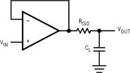
The LMV791 and LMV792 can directly drive up to 120 pF in unity gain without oscillation. The unity gain follower is the most sensitive configuration to capacitive loading. Direct capacitive loading reduces the phase margin of amplifiers. The combination of the output impedance of the amplifier and the capacitive load induces phase lag. This results in either an underdamped pulse response or oscillation. To drive a heavier capacitive load, the circuit in Figure 46 can be used.
In Figure 46, the isolation resistor RISO and the load capacitor CL form a pole to increase stability by adding more phase margin to the overall system. The desired performance depends on the value of RISO. The bigger the RISO resistor value, the more stable VOUT will be. Increased RISO would, however, result in a reduced output swing and short circuit current.
 Figure 46. Isolation of CL to Improve Stability
7.4.2 Input Capacitance and Feedback Circuit Elements
The LMV791 family has a very low input bias current (100 fA) and a low 1/f noise corner frequency (400 Hz), which makes it ideal for sensor applications. However, to obtain this performance a large CMOS input stage is used, which adds to the input capacitance of the operational amplifier, CIN. Though this does not affect the DC and low frequency performance, at higher frequencies the input capacitance interacts with the input and the feedback impedances to create a pole, which results in lower phase margin and gain peaking. This can be controlled by being selective in the use of feedback resistors, as well as by using a feedback capacitance, CF. For example, in the inverting amplifier shown in Figure 47, if CIN and CF are ignored and the open-loop gain of the operational amplifier is considered infinite then the gain of the circuit is −R2/R1. An operational amplifier, however, usually has a dominant pole, which causes its gain to drop with frequency. Hence, this gain is only valid for DC and low frequency. To understand the effect of the input capacitance coupled with the non-ideal gain of the operational amplifier, the circuit needs to be analyzed in the frequency domain using a Laplace transform.
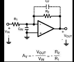 Figure 47. Inverting Amplifier
For simplicity, the operational amplifier is modeled as an ideal integrator with a unity gain frequency of A0. Hence, its transfer function (or gain) in the frequency domain is A0/s. Solving the circuit equations in the frequency domain, ignoring CF for the moment, results in an expression for the gain shown in Equation 1.
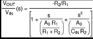
It can be inferred from the denominator of the transfer function that it has two poles, whose expressions can be obtained by solving for the roots of the denominator and are shown in Equation 2.

Equation 2 shows that as the values of R1 and R2 are increased, the magnitude of the poles, and hence the bandwidth of the amplifier, is reduced. This theory is verified by using different values of R1 and R2 in the circuit shown in Figure 46 and by comparing their frequency responses. In Figure 48 the frequency responses for three different values of R1 and R2 are shown. When both R1 and R2 are 1 kΩ, the response is flattest and widest; whereas, it narrows and peaks significantly when both their values are changed to 10 kΩ or 30 kΩ. So it is advisable to use lower values of R1 and R2 to obtain a wider and flatter response. Lower resistances also help in high-sensitivity circuits because they add less noise.
A way of reducing the gain peaking is by adding a feedback capacitance CF in parallel with R2. This introduces another pole in the system and prevents the formation of pairs of complex conjugate poles which cause the gain to peak. Figure 49 shows the effect of CF on the frequency response of the circuit. Adding a capacitance of 2 pF removes the peak, while a capacitance of 5 pF creates a much lower pole and reduces the bandwidth excessively.
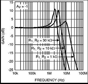 Figure 48. Gain Peaking Caused by Large R1, R2
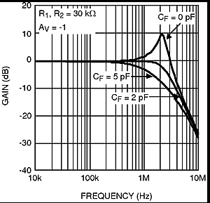 Figure 49. Gain Peaking Eliminated by CF