SNAS601G August 2012 – September 2014 LMX2581
PRODUCTION DATA.
- 1 Features
- 2 Applications
- 3 Description
- 4 Simplified Schematic
- 5 Revision History
- 6 Pin Configuration and Functions
- 7 Specifications
-
8 Detailed Description
- 8.1 Overview
- 8.2 Functional Block Diagram
- 8.3
Feature Description
- 8.3.1 Typical Performance Characteristics
- 8.3.2 Impact of Temperature on VCO Phase Noise
- 8.3.3 OSCin INPUT and OSCin Doubler
- 8.3.4 R Divider
- 8.3.5 PLL N Divider And Fractional Circuitry
- 8.3.6 PLL Phase Detector and Charge Pump
- 8.3.7 External Loop Filter
- 8.3.8 Low Noise, Fully Integrated VCO
- 8.3.9 Programmable VCO Divider
- 8.3.10 0-Delay Mode
- 8.3.11 Programmable RF Output Buffers
- 8.3.12 Fastlock
- 8.3.13 Lock Detect
- 8.3.14 Part ID and Register Readback
- 8.3.15 Optimization of Spurs
- 8.4 Device Functional Modes
- 8.5 Programming
- 8.6
Register Maps
- 8.6.1
Programming Word Descriptions
- 8.6.1.1 Register R15
- 8.6.1.2 Register R13
- 8.6.1.3 Registers R10, R9, and R8
- 8.6.1.4 Register R7
- 8.6.1.5 Register R6
- 8.6.1.6
Register R5
- 8.6.1.6.1 OUT_LDEN — Mute Outputs Based on Lock Detect
- 8.6.1.6.2 OSC_FREQ[2:0] — OSCin Frequency for VCO Calibration
- 8.6.1.6.3 BUFEN_DIS - Disable for the BUFEN Pin
- 8.6.1.6.4 VCO_SEL_MODE — Method of Selecting Internal VCO Core
- 8.6.1.6.5 OUTB_MUX — Mux for RFoutB
- 8.6.1.6.6 OUTA_MUX — Mux for RFoutA
- 8.6.1.6.7 0_DLY - Zero Delay Mode
- 8.6.1.6.8 MODE[1:0] — Operating Mode
- 8.6.1.6.9 PWDN_MODE - Powerdown Mode
- 8.6.1.6.10 RESET - Register Reset
- 8.6.1.7 Register R4
- 8.6.1.8 Register R3
- 8.6.1.9 Register R2
- 8.6.1.10 Register R1
- 8.6.1.11 Register R0
- 8.6.1
Programming Word Descriptions
- 9 Application and Implementation
- 10Power Supply Recommendations
- 11Layout
- 12Device and Documentation Support
- 13Mechanical, Packaging, and Orderable Information
Package Options
Mechanical Data (Package|Pins)
- RTV|32
Thermal pad, mechanical data (Package|Pins)
- RTV|32
Orderable Information
9 Application and Implementation
NOTE
Information in the following applications sections is not part of the TI component specification, and TI does not warrant its accuracy or completeness. TI’s customers are responsible for determining suitability of components for their purposes. Customers should validate and test their design implementation to confirm system functionality.
9.1 Application Information
The LMX2581 can be used in a broad class of applications. In general, they tend to fall in the categories where the output frequency is a nicely related input frequency and those that require fractional mode. The following schematic generally applies to most applications.
9.2 Typical Applications
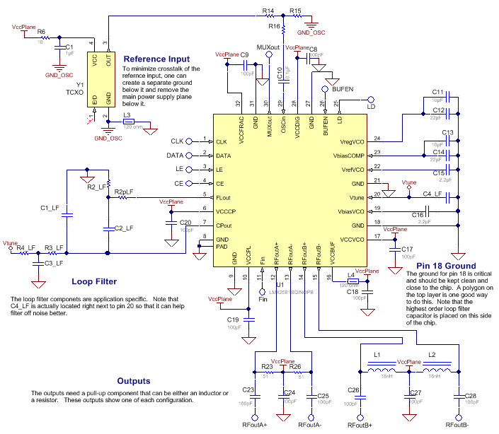 Figure 21. Typical Schematic
9.2.1 Clocking Application
When the output and input frequencies are nicely related, the LMX2581 can often achieve this in integer mode. In integer mode, fractional spurs and noise are much less of a concern, so higher phase detector frequency and wider loop bandwidth are typically used for optimal phase noise performance.
9.2.1.1 Design Requirements
For this example, consider a design for a fixed 1500 MHz output clock to be generated from a 100 MHz input clock. Good close in phase noise and maximizing the output power are desired in this particular example
9.2.1.2 Detailed Design Procedure
For this kind of application, the design goal is typically to minimize the jitter.
| PARAMETER | VALUE | REASON for CHOOSING |
|---|---|---|
| Fout | 1500 MHz | This parameter was given. |
| Fosc | 100 MHz | This parameter was given. |
| Fpd | 200 MHz | Choose a highest possible phase detector frequency. There are no fractional spurs and this increases the value of C1 |
| Fvco | 3000 MHz | The VCO needs to be a multiple of 1500 MHz, which restricts it to be 3000 MHz. |
| Kpd | 31x | This maximizes the C1 capacitor and also the phase noise |
| Loop Bandwidth | 256 kHz | Theoretically, optimal jitter is obtained by choosing the loop bandwidth to the frequency where the open loop PLL and closed loop VCO noise are equal, which would be about 250 kHz. The phase margin is typically chosen around 70 degrees, but is chosen to be 50 degrees to increase the value of the C1 capacitor to be at least 1 nF to reduce VCO phase noise degradation. |
| Phase Margin | 50 deg | |
| OUT_A_PWR | 45 | This yields the maximum output power. |
| C1 | 1 nF | Calculated with TI clock design software |
| C2 | 6.8 nF | |
| R2 | 270 Ω | |
| Pull-Up Component | 18 nH Inductor | This gives maximum output power. |
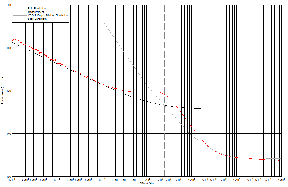
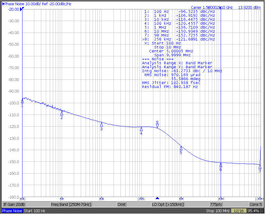
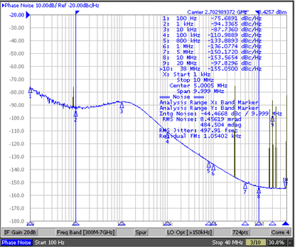
9.2.1.3 Application Curves
Figure 22 is an example of the performance that one might see for an application like this. The achieved results show an output power of about 14 dBm (single-ended) and a jitter from 100 Hz to 10 MHz of 100 fs. Note that the output power is higher than +12 dBm as claimed in the electrical specifications because this is at a lower frequency than 2.7 GHz.
9.2.2 Fractional PLL Application
For applications where the output frequency is not always related nicely to the input frequency, lowering the loop bandwidth and reducing the phase detector frequency can often improve spurs at the cost of in-band phase noise.
9.2.2.1 Design Requirements
Consider generating 1880 to 3760 MHz from a 100 MHz input frequency with a channel spacing of 200 kHz. This is the situation similar that was used for the EVM board.
9.2.2.2 Detailed Design Procedure
| PARAMETER | VALUE | REASON for CHOOSING |
|---|---|---|
| Fout | 1880 - 3760 MHz | This parameter was given. |
| Fosc | 100 MHz | This parameter was given. |
| Fpd | 25 MHz | By trial and error and experimenting with the clock design tool, we see that this gives a good trade-off between the integer boundary spur and phase noise. |
| Loop Bandwidth | 28.7 KHz | This is around where the PLL and VCO noise meet. The VCO is at 2700 MHz |
| Kpd | 31x | Choose the highest charge pump gain to maximize the capacitor next to the VCO. |
| C1_LF | 1.8 nF | The loop filter can be calculated with the clock design tool. Note that we need to keep the loop bandwidth not too wide so that the capacitor next to the VCO is larger. Also, it is put in C4_LF spot, not C3_LF spot. Both are electrically equivalent, but layoutwise, C4_LF makes more sense. See the board layout in sections to come. |
| C2_LF | 56 nF | |
| C3_LF | Open | |
| C4_LF | 3.3 nF | |
| R2_LF | 390 Ω | |
| R3_LF | 270 Ω | |
| R4_LF | 0 Ω | |
| OUT_A_PWR | 30 | This combination of pull-up component and output power settings yields optimal noise floor. |
| Pull-Up Component | 18 nH Inductor |
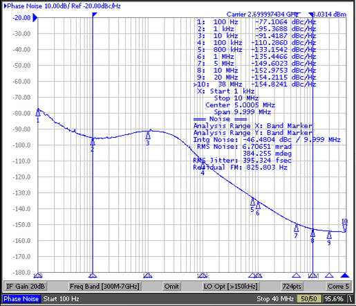
9.2.2.3 Application Curves
9.3 Do's and Don'ts
| CATEGORY | DO | DON'T | WHY |
|---|---|---|---|
| Output Pull-Up Components | Place pull-up components close to RFoutA and RFoutB | Go through a Via before getting to the pull-up component. | The output impedance is determined by this component and if it is far away, there will be loss in output power. |
| Fractional Spurs |
|
|
Fractional spurs can have more than one mechanism, especially the integer boundary spur. |
| Dithering |
|
Use on simple fractions . | Dithering is very effective in eliminating some spurs, but useless for eliminating others. Dithering adds PLL phase noise, so it should be only used for appropriate situations. |
| VbiasCOMP and VbiasVCO | Put as much capacitance as possible, up to 32 µF |
|
This capacitance impacts the VCO phase noise. |