SNAS601G August 2012 – September 2014 LMX2581
PRODUCTION DATA.
- 1 Features
- 2 Applications
- 3 Description
- 4 Simplified Schematic
- 5 Revision History
- 6 Pin Configuration and Functions
- 7 Specifications
-
8 Detailed Description
- 8.1 Overview
- 8.2 Functional Block Diagram
- 8.3
Feature Description
- 8.3.1 Typical Performance Characteristics
- 8.3.2 Impact of Temperature on VCO Phase Noise
- 8.3.3 OSCin INPUT and OSCin Doubler
- 8.3.4 R Divider
- 8.3.5 PLL N Divider And Fractional Circuitry
- 8.3.6 PLL Phase Detector and Charge Pump
- 8.3.7 External Loop Filter
- 8.3.8 Low Noise, Fully Integrated VCO
- 8.3.9 Programmable VCO Divider
- 8.3.10 0-Delay Mode
- 8.3.11 Programmable RF Output Buffers
- 8.3.12 Fastlock
- 8.3.13 Lock Detect
- 8.3.14 Part ID and Register Readback
- 8.3.15 Optimization of Spurs
- 8.4 Device Functional Modes
- 8.5 Programming
- 8.6
Register Maps
- 8.6.1
Programming Word Descriptions
- 8.6.1.1 Register R15
- 8.6.1.2 Register R13
- 8.6.1.3 Registers R10, R9, and R8
- 8.6.1.4 Register R7
- 8.6.1.5 Register R6
- 8.6.1.6
Register R5
- 8.6.1.6.1 OUT_LDEN — Mute Outputs Based on Lock Detect
- 8.6.1.6.2 OSC_FREQ[2:0] — OSCin Frequency for VCO Calibration
- 8.6.1.6.3 BUFEN_DIS - Disable for the BUFEN Pin
- 8.6.1.6.4 VCO_SEL_MODE — Method of Selecting Internal VCO Core
- 8.6.1.6.5 OUTB_MUX — Mux for RFoutB
- 8.6.1.6.6 OUTA_MUX — Mux for RFoutA
- 8.6.1.6.7 0_DLY - Zero Delay Mode
- 8.6.1.6.8 MODE[1:0] — Operating Mode
- 8.6.1.6.9 PWDN_MODE - Powerdown Mode
- 8.6.1.6.10 RESET - Register Reset
- 8.6.1.7 Register R4
- 8.6.1.8 Register R3
- 8.6.1.9 Register R2
- 8.6.1.10 Register R1
- 8.6.1.11 Register R0
- 8.6.1
Programming Word Descriptions
- 9 Application and Implementation
- 10Power Supply Recommendations
- 11Layout
- 12Device and Documentation Support
- 13Mechanical, Packaging, and Orderable Information
Package Options
Mechanical Data (Package|Pins)
- RTV|32
Thermal pad, mechanical data (Package|Pins)
- RTV|32
Orderable Information
6 Pin Configuration and Functions
32-Pin
DAP Package
(Top View)
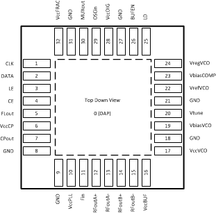
Pin Functions
| PIN | TYPE | DESCRIPTION | |
|---|---|---|---|
| NUMBER | NAME | ||
| 0 | DAP | GND | The DAP should be grounded. |
| 1 | CLK | Input | MICROWIRE Clock Input. High Impedance CMOS input. |
| 2 | DATA | Input | MICROWIRE Data. High Impedance CMOS input. |
| 3 | LE | Input | MICROWIRE Latch Enable. High Impedance CMOS input. |
| 4 | CE | Input | Chip Enable Pin. |
| 5 | FLout | Output | Fastlock Output. This can switch in an external resistor to the loop filter during locking to improve lock time. |
| 6 | VccCP | Supply | Charge Pump Supply. |
| 7 | CPout | Output | Charge Pump Output. |
| 8 | GND | GND | Ground for the Charge Pump. |
| 9 | GND | GND | Ground for the N and R divider. |
| 10 | VccPLL | Supply | Supply for the PLL. |
| 11 | Fin | Input | High frequency input pin for an external VCO. Leave Open or Ground if not used. |
| 12 | RFoutA+ | Output | Differential divided output. For single-ended operation, terminate the complimentary side with a load equivalent to the load at this Pin. |
| 13 | RFoutA- | Output | Differential divided output. For single-ended operation, terminate the complimentary side with a load equivalent to the load at this pin. |
| 14 | RFoutB+ | Output | Differential divided output. For single-ended operation, terminate the complimentary side with a load equivalent to the load at this pin. |
| 15 | RFoutB- | Output | Differential divided output. For single-ended operation, terminate the complimentary side with a load equivalent to the load at this pin. |
| 16 | VccBUF | Supply | Supply for the Output Buffer. |
| 17 | VccVCO | Supply | Supply for the VCO. |
| 18 | GND | GND | Ground Pin for the VCO. This can be attached to the regular ground. Ensure a solid trace connects this pin to the bypass capacitors on pins 19, 23, and 24. |
| 19 | VbiasVCO | Output | Bias circuitry for the VCO. Place a 2.2 µF capacitor to GND (Preferably close to Pin 18). |
| 20 | Vtune | Input | VCO tuning voltage input. See the functional description regarding the minimum capacitance to put at this pin. |
| 21 | GND | GND | VCO ground. |
| 22 | VrefVCO | Output | VCO capacitance. Place a capacitor to GND (Preferably close to Pin 18). This value should be between 5% and 10% of the capacitance at pin 24. Recommended value is 1 µF. |
| 23 | VbiasCOMP | Output | VCO bias voltage temperature compensation circuit. Place a minimum 10 µF capacitor to GND (Preferably close to Pin 18). If it is possible, use more capacitance to slightly improve VCO phase noise. |
| 24 | VregVCO | Output | VCO regulator output. Place a minimum 10 µF capacitor to GND (Preferably close to Pin 18). If it is possible, use more capacitance to slightly improve VCO phase noise. |
| 25 | LD | Output | Multiplexed output that can perform lock detect, PLL N and R counter outputs, Readback, and other diagnostic functions. |
| 26 | BUFEN | Input | Enable pin for the RF output buffer. If not used, this can be overwritten in software. |
| 27 | GND | GND | Digital Ground. |
| 28 | VccDIG | Supply | Digital Supply. |
| 29 | OSCin | Input | Reference input clock. |
| 30 | MUXout | Output | Multiplexed output that can perform lock detect, PLL N and R counter outputs, Readback, and other diagnostic functions.. |
| 31 | GND | GND | Ground for the fractional circuitry. |
| 32 | VccFRAC | Vcc | Supply for the fractional circuitry. |