SNAS601G August 2012 – September 2014 LMX2581
PRODUCTION DATA.
- 1 Features
- 2 Applications
- 3 Description
- 4 Simplified Schematic
- 5 Revision History
- 6 Pin Configuration and Functions
- 7 Specifications
-
8 Detailed Description
- 8.1 Overview
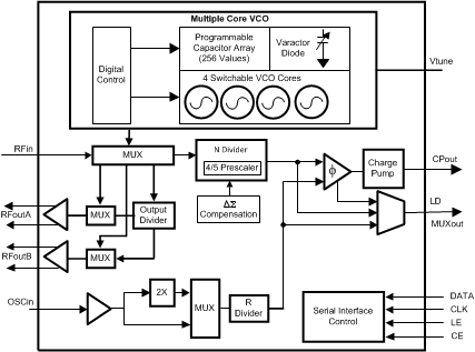
- 8.2 Functional Block Diagram
- 8.3
Feature Description
- 8.3.1 Typical Performance Characteristics
- 8.3.2 Impact of Temperature on VCO Phase Noise
- 8.3.3 OSCin INPUT and OSCin Doubler
- 8.3.4 R Divider
- 8.3.5 PLL N Divider And Fractional Circuitry
- 8.3.6 PLL Phase Detector and Charge Pump
- 8.3.7 External Loop Filter
- 8.3.8 Low Noise, Fully Integrated VCO
- 8.3.9 Programmable VCO Divider
- 8.3.10 0-Delay Mode
- 8.3.11 Programmable RF Output Buffers
- 8.3.12 Fastlock
- 8.3.13 Lock Detect
- 8.3.14 Part ID and Register Readback
- 8.3.15 Optimization of Spurs
- 8.4 Device Functional Modes
- 8.5 Programming
- 8.6
Register Maps
- 8.6.1
Programming Word Descriptions
- 8.6.1.1 Register R15
- 8.6.1.2 Register R13
- 8.6.1.3 Registers R10, R9, and R8
- 8.6.1.4 Register R7
- 8.6.1.5 Register R6
- 8.6.1.6
Register R5
- 8.6.1.6.1 OUT_LDEN — Mute Outputs Based on Lock Detect
- 8.6.1.6.2 OSC_FREQ[2:0] — OSCin Frequency for VCO Calibration
- 8.6.1.6.3 BUFEN_DIS - Disable for the BUFEN Pin
- 8.6.1.6.4 VCO_SEL_MODE — Method of Selecting Internal VCO Core
- 8.6.1.6.5 OUTB_MUX — Mux for RFoutB
- 8.6.1.6.6 OUTA_MUX — Mux for RFoutA
- 8.6.1.6.7 0_DLY - Zero Delay Mode
- 8.6.1.6.8 MODE[1:0] — Operating Mode
- 8.6.1.6.9 PWDN_MODE - Powerdown Mode
- 8.6.1.6.10 RESET - Register Reset
- 8.6.1.7 Register R4
- 8.6.1.8 Register R3
- 8.6.1.9 Register R2
- 8.6.1.10 Register R1
- 8.6.1.11 Register R0
- 8.6.1
Programming Word Descriptions
- 9 Application and Implementation
- 10Power Supply Recommendations
- 11Layout
- 12Device and Documentation Support
- 13Mechanical, Packaging, and Orderable Information
Package Options
Mechanical Data (Package|Pins)
- RTV|32
Thermal pad, mechanical data (Package|Pins)
- RTV|32
Orderable Information
8 Detailed Description
8.1 Overview
The LMX2581 is a synthesizer, consisting of a reference input and R divider, phase detector and charge pump, VCO and high frequency fractional (N) divider, and two programmable output buffers. The device requires external components for the loop filter and output buffers, which are application dependent.
Based on the oscillator input frequency (fOSC), PLL R divider value (PLL_R), PLL N Divider Value (PLL_N), Fractional Numerator (PLL_NUM), Fractional Denominator (PLL_DEN), and VCO divider value (VCO_DIV), the output frequency of the LMX2581 (fOUT) can be determined as follows:
8.2 Functional Block Diagram
8.3 Feature Description
8.3.1 Typical Performance Characteristics
8.3.1.1 Phase Noise Typical Performance Plot Explanations
Figure 2 shows 2700 MHz output and a 100 MHz phase detector frequency. The modeled noises (Flat, Flicker, and Total) are calculated from the normalized -229 dBc/Hz figure of merit and the -120.8 dBc/Hz normalized 1/f noise from the electrical table. After 200 kHz, the loop filter dynamics cause the noise to increase sharply.
Figure 3 shows the relative changes with the normalized PLL noise and figure of merit as a function of charge pump gain. The PLL phase noise changes as a function of the charge pump gain.
Figure 4 shows the phase noise for a filter optimized for spurs with a 20 MHz phase detector and running in fractional mode with strong dithering. Due to the narrower loop bandwidth, the impact of the VCO phase noise inside the loop bandwidth is in the 1 to 10 kHz region.
In Figure 5, the loop filter was optimized for RMS jitter. This was in fractional mode with a phase detector of 200 MHz and uses the First Order Modulator.
In Figure 6, the output divider noise floor only applies when the output divider is not bypassed and depends mainly on output frequency, not the actual divide value.
8.3.1.2 Other Typical Performance Plot Characteristics Explanations
Figure 7 shows a frequency change of 1880 MHz to 3760 MHz with Fosc = Fpd = 100 MHz. If the VCO3 is selected as the starting VCO with VCO_CAPCODE=127, digital calibration time is closer to 115 µs. If VCO4 is selected as the starting VCO with VCO_CAPCODE=15, the calibration time is greatly shortened to something of the order of 5 µs.
Figure 8 was measured with a board with very short traces. Only one of the differential outputs is routed.
In Figure 9, the output impedance is mainly determined by the pull-up component used at lower frequencies. For the resistor, it is 51 Ω up to about 2 GHz, where the impedance of the device starts to dominate. For the inductor it increases with frequency and then reaches a resonance frequency before coming down. These behaviors are specific to the pull-up component. These impedance plots match the conditions that were used to measure output power.
In Figure 12, the OSCin input sensitivity for a sine wave. The voltage has no impact and the temperature only has a slight impact. Enabling the doubler limits the performance
In Figure 13, For lower frequencies, the magnitude of the OSCin input impedance can be considered high relative to 50 Ω. At higher frequencies, it is not as high and a resistive pad may be better than a simple shunt 50 Ω resistor for matching.
8.3.2 Impact of Temperature on VCO Phase Noise
The phase noise specifications for the VCO in Electrical Characteristics are for a narrow loop bandwidth at room temperature. If the temperature is changed, Table 1 gives an approximation on how the VCO phase noise is impacted. For instance, if one was to lock the PLL at -40°C and then measure the phase noise at 1 MHz offset, the phase noise would typically be of the order of 2 dB better than if it was locked and measured at 25°C. If the PLL is locked at -40°C and then the temperature was to drift to 85°C, then the phase noise at 1 MHz offset would typically be about 2 dB worse than it would be if it was locked and measured at 25°C. These numbers are only approximations and may change between devices and over VCO cores slightly.
Table 1. Approximate Change in VCO Phase Noise vs. Temperature and Temperature Drift in dB
| STARTING TEMPERATURE | FINAL TEMPERATURE | OFFSET | ||||
|---|---|---|---|---|---|---|
| 10 kHz | 100 kHz | 1 MHz | 10 MHz | 40 MHz | ||
| -40°C | -40°C | -2 | -1 | -2 | -2 | 0 |
| 25°C | -1 | 0 | 0 | -1 | 0 | |
| 85°C | -3 | 2 | 2 | -0 | 0 | |
| 25°C | -40°C | -1 | -1 | 0 | -1 | 0 |
| 25°C | These are all zero because all measurements are relative to this row. | |||||
| 85°C | -3 | 2 | 2 | 0 | 0 | |
| 85°C | -40°C | -4 | -2 | -2 | 0 | 0 |
| 25°C | -1 | 0 | 0 | -2 | 0 | |
| 85°C | -2 | 2 | 2 | 0 | 0 | |
8.3.3 OSCin INPUT and OSCin Doubler
The OSCin pin is driven with a single-ended signal which is used as a frequency reference. Before the OSCin frequency reaches the phase detector, it may be doubled with the OSCin doubler and/or divided with the PLL R divider.
Because the OSCin signal is used as a clock for the VCO calibration, the OSC_FREQ word needs to be programmed correctly and a proper signal needs to be applied at the OSCin pin at the time of programming the R0 register in order for the VCO calibration to properly work. Higher slew rates tend to yield the best fractional spurs and phase noise, so a square wave signal is best for OSCin. If using a sine wave, higher frequencies tend to yield better phase noise and fractional spurs due to their higher slew rates. The OSCin pin has high impedance, so for optimal performance, it is recommended to use either a shunt resistor or resistive pad to make sure that the impedances looking towards and away from the device input are both close to 50 Ω.
8.3.4 R Divider
The R divider divides the OSCin frequency down to the phase detector frequency. With this device, it is possible to use both the doubler and the R divider at the same time.
8.3.5 PLL N Divider And Fractional Circuitry
The N divider includes fractional compensation and can achieve any fractional denominator (PLL_DEN) from 1 to 4,194,303. The integer portion, PLL_N, is the whole part of the N divider value and the fractional portion, PLL_NUM / PLL_DEN, is the remaining fraction. PLL_N, PLL_NUM, and PLL_DEN are software programmable. So in general, the total N divider value, N, is determined by: N = PLL_N + PLL_NUM / PLL_DEN. The order of the delta sigma modulator is programmable from integer mode to third order. There are also several dithering modes that are also programmable. In order to make the fractional spurs consistent, the modulator is reset any time that the R0 register is programmed.
8.3.5.1 Programmable Dithering Levels
If used appropriately, dithering may be used to reduce sub-fractional spurs, but if used inappropriately, it can actually create spurs and increase phase noise. Table 2 provides guidelines for the use of dithering based on the fractional denominator, after the fraction is reduced to lowest terms.
Table 2. Dithering Recommendations
| FRACTION | DITHERING RECOMMENDATION |
COMMENTS |
|---|---|---|
| Fractional Numerator = 0 | Disable Dithering | This is often the worst case for spurs, which can actually be turned into the best case by simply disabling dithering. This will have performance that is similar to integer mode. |
| Equivalent Denominator < 20 | Disable Dithering | These fractions are not well randomized and dithering will likely create phase noise and spurs. |
| Equivalent Denominator is not divisible by 2 or 3 | Disable Dithering | There will be no sub-fractional spurs, so dithering is likely not to be very effective |
| Equivalent Denominator > 200 and is divisible by 2 or 3 | Consider Dithering | Dithering may help reduce the sub-fractional spurs, but understand it may degrade the PLL phase noise. |
In general, dithering is likely to cause more harm than good for poorly randomized fractions like 1/2. There are situations when dithering does make sense and when it is used, it is recommended to adjust the PFD_DLY word accordingly to compensate for this.
8.3.5.2 Programmable Delta Sigma Modulator Order
The fractional modulator order is programmable, which gives the opportunity to better optimize phase noise and spurs. Theoretically, higher order modulators push out phase noise to farther offsets, as described in Table 3.
Table 3. Choosing the Fractional Modulator Order
| MODULATOR ORDER | APPLICATIONS |
|---|---|
| Integer Mode (Order = 0) |
If the fractional numerator is zero, it is best to run the device in integer mode to minimize phase noise and spurs. |
| First Order Modulator | When the equivalent fractional denominator is 6 or less, the first order modulator theoretically has lower phase noise and spurs, so it always makes sense in these situations. When the fractional denoninator is between 6 and about 20, consider using the first order modulator because the spurs might be far enough outside the loop bandwidth that they will be filtered. The first order modulator also does not create any sub-fractional spurs or phase noise. |
| 2nd and 3rd Order Modulators | The choice between 2nd and 3rd order modulator tends to be a little more application specific. If the fractional denominator is not divisible by 3, then the 2nd and 3rd order modulators will have spurs in the same offsets, so the 3rd is generally better for spurs. However, if stronger levels of dithering is used, the 3rd order modulator will create more close-in phase noise than the 2nd order modulator |
Figure 14 and Figure 15 give an idea of the theoretical impact of the delta sigma modulator order on the shaping of the phase noise and spurs. In terms of phase noise, this is what one would theoretically expect if strong dithering was used for a well-randomized fraction. Dithering can be set to different levels or even shut off and the noise can be eliminated. In terms of spurs, they can change based on fraction, but they will theoretically pushed out to higher phase detector frequencies. However, one must be aware that these are just THEORETICAL graphs and for offsets that on the order of less than 5% of the phase detector frequency, other factors can impact the noise and spurs. In Figure 14, the curves all cross at 1/6th of the phase detector frequency and that this transfer function peaks at half of the phase detector frequency, which is assumed to be well outside the loop bandwidth. Figure 15 shows the impact of the phase detector frequency on the modulator noise.
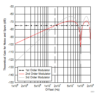 Figure 14. Theoretical Delta Sigma Noise Shaping for a 100 MHz Phase Detector Frequency
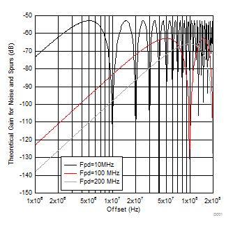 Figure 15. Theoretical Delta Sigma Noise Shaping for 3rd Order Modulator
For lower offsets, the actual noise added by the delta sigma modulator may be higher than the theoretical values shown due to nonlinearity of the phase detector. This noise floor can vary with the modulator order, phase detector frequency, and PFD_DLY word setting as shown in the following table, which shows the phase noise at 10 kHz offset for a frequency close to 2801 MHz with a well randomized fraction and strong dithering. The phase noise in integer mode is also shown for comparison purposes.
Table 4. Impact of PFD_DLY, Modulator Order, and Phase Detector Frequency on Modulator Noise Floor
| INTEGER | 2nd ORDER MODULATOR | 3rd ORDER MODULATOR | ||||||||||
|---|---|---|---|---|---|---|---|---|---|---|---|---|
| PFD_ DLY |
Fpd= 25 MHz |
Fpd= 50MHz |
Fpd= 100 MHz |
Fpd= 200 MHz |
Fpd= 25 MHz |
Fpd= 50MHz |
Fpd= 100 MHz |
Fpd= 200 MHz |
Fpd= 25 MHz |
Fpd= 50MHz |
Fpd= 100 MHz |
Fpd= 200 MHz |
| 0 | -106.7 | -109.5 | -111.4 | -111.0 | -106.3 | -108.8 | -110.6 | -111.0 | -84.4 | -87.5 | -90.1 | -93.8 |
| 1 | -106.2 | -108.8 | -110.6 | -110.9 | -106.5 | -108.4 | -110.1 | -110.0 | -88.3 | -91.3 | -93.6 | -98.5 |
| 2 | -106.0 | -108.3 | -109.7 | -110.1 | -105.6 | -108.3 | -109.2 | -110.1 | -92.9 | -96.1 | -98.1 | -102.8 |
| 3 | -106.0 | -108.2 | -109.4 | -109.9 | -105.3 | -107.9 | -109.2 | -109.8 | -99.2 | -101.8 | -102.6 | -105.4 |
| 4 | -105.6 | -107.7 | -109.4 | -110.0 | -105.1 | -107.5 | -108.7 | -109.3 | -103.0 | -105.4 | -105.8 | -106.2 |
| 5 | -105.5 | -107.6 | -108.8 | -110.1 | -105.6 | -107.4 | -108.6 | -109.0 | -101.4 | -104.0 | -103.7 | -105.5 |
| 6 | -105.1 | -107.3 | -108.5 | -109.3 | -104.6 | -107.0 | -107.8 | -109.1 | -98.4 | -101.6 | -102.7 | -102.9 |
| 7 | -104.8 | -106.8 | -108.2 | -105.9 | -104.6 | -106.2 | -107.4 | -108.7 | -97.1 | -100.6 | -102.1 | -100.2 |
8.3.6 PLL Phase Detector and Charge Pump
The phase detector compares the outputs of the R and N dividers and generates a correction current corresponding to the phase error. This charge pump current is software programmable to many different levels. The phase detector frequency, fPD, can be calculated as follows:
The charge pump outputs a correction current into the loop filter, which is implemented with external components. The gain of the charge pump is programmable to 32 different levels with the CPG word and the PFD_DLY word can adjust the minimum on time that the charge pump comes on for.
8.3.7 External Loop Filter
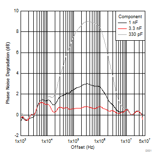
The LMX2581 requires an external loop filter which is application-specific and can be configured by consulting LMX2581 Tools and Software). For the LMX2581, it matters what impedance is seen from the Vtune pin looking outwards. This impedance is dominated by the component C3_LF for a third order filter or C1_LF for a second order filter (R3_LF=C3_LF=0). If there is at least 3.3 nF for the capacitance that is shunt with this pin, the VCO phase noise will be close to the best it can be. If there is less, the VCO phase noise in the 100k to 1MHz region. In cases where 3.3 nF might restrict the loop bandwidth to be too narrow, it might make sense to violate this restriction a little and sacrifice some VCO phase noise in order to get a wider loop bandwidth.
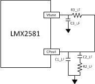 Figure 16. Typical Loop Filter
8.3.8 Low Noise, Fully Integrated VCO
The VCO takes the voltage from the loop filter and converts this into a frequency. The VCO frequency is related to the other frequencies and divider values as follows: fVCO = fPD × N = fOSCin × OSC_2X × N / R. The VCO is fully integrated, including the tank circuitry.
In order to the reduce the VCO tuning gain and therefore improve the VCO phase noise performance, the internal VCO is actually made of VCO cores working as one. These cores starting from lowest frequency to highest frequency are VCO 1, VCO 2, VCO 3, and VCO 4. Each VCO core has 256 different frequency bands. Band 255 is the lowest frequency and Band 0 is the highest This creates the need for frequency calibration in order to determine the correct VCO core and correct frequency band in that VCO core. The frequency calibration routine is activated any time that the R0 register is programmed with the NO_FCAL bit equal to zero. In order for this frequency calibration to work properly, the OSC_FREQ word needs to be set to the correct setting. The VCO_SEL word allows the user to suggest a particular VCO core for the device to choose, which is useful for optimizing fractional spurs and minimizing lock time.
Table 5. Approximate (NOT Ensured) VCO Core Frequency Ranges
| VCO CORE | APPROXIMATE FREQUENCY RANGE |
|---|---|
| VCO 1 | 1800 to 2270 MHz |
| VCO 2 | 2135 to 2720 MHz |
| VCO 3 | 2610 to 3220 MHz |
| VCO 4 | 3075 to 3800 MHz |
8.3.8.1 VCO Digital Calibration
When the frequency is changed, the digital VCO goes through the following VCO calibration:
- Depending on the status of the VCO_SEL word, the starting VCO core is selected.
- The algorithm starts counting at the default band in this core as determined by the VCO_CAPCODE value.
- The VCO increments or decrements the CAPCODE based on the what the actual VCO output is compared to the target VCO output.
- Repeat step 3 until either the VCO is locked or the VCO is at VCO_CAPCODE = 0 or 255
- If not locked, then choose the next appropriate VCO if possible and return to step 3. If not possible, the calibration is terminated.
A good starting point is to set VCO_SEL = 2 for VCO 3 and set VCO_SEL_MODE = 1 to start at the selected core. If there is the potential of switching the VCO from a frequency above 3 GHz directly to a frequency below 2.2 GHz, VCO_SEL_MODE can not be set to 0. In this case, VCO_SEL_MODE can still be set to 1 to select a starting core, but the starting core specified by VCO_SEL can not be VCO 4.
The digital calibration time can be improved dramatically by giving the VCO guidance regarding which VCO core and which VCO_CAPCODE to start using. Even if the wrong VCO core is chosen, which could happen near the boundary of two cores, the calibration time is improved. For situations where the frequency change is small, the device can be programmed to automatically start at the last VCO core used. For applications where the frequency change is relatively small, the best VCO calibration time can often be achieved by setting the VCO_SEL_MODE to choose the last VCO core that was used.
8.3.9 Programmable VCO Divider
The VCO divider can be programmed to even values from 2 to 38 as well as bypassed by either one or both of the RFout outputs. When the zero delay mode is not enabled, the VCO divider is not in the feedback path between the VCO and the PLL and therefore has no impact on the PLL loop dynamics. After this programmable divider is changed, it may be beneficial to reprogram the R0 register to recalibrate the VCO. The frequency at the RFout pin is related to the VCO frequency and divider value, VCO_DIV, as follows:
When this divider is enabled, there will be some far-out phase noise contribution to the VCO noise.
When changing to a VCO_DIV value of 4, either from a state of VCO_DIV=2 or OUTx_MUX = 0, it is necessary to program VCO_DIV first to a value of 6, then to a value of 4. This holds for no other VCO_DIV value and is not necessary if the VCO frequency (but not VCO_DIV) is changing.
8.3.10 0–Delay Mode
When the VCO divider is used, an ambiguous phase relationship is created between the OSCin and RFout pins. 0–Delay mode can be enabled to eliminate this ambiguity.
When this mode is used, special care needs to be taken because it does interfere with the VCO calibration if not done correctly. The correct way to use 0–Delay mode is as follows:
- If N is not divisible by VCO_DIV, reduce the phase detector frequency to make it so.
- Program as normal and lock the PLL.
- Program the NO_FCAL =1.
- Program 0_DLY = 1. This will cause the PLL to lose lock.
- Program the PLL_N value with PLL_N* / VCO_DIV, where PLL_N* is the original value.
- The PLL should now be locked in zero delay mode.
8.3.11 Programmable RF Output Buffers
The output states of the RFoutA and RFoutB pins are controlled by the BUFEN pin as well as the BUFEN_DIS programming bit. If the pin is powered up, then output power can be programmed to various levels with the OUTx_PWR words.
Table 6. Output States of the RFoutA and RFoutB Pins
| OUTA_PD OUTB_PD |
BUFEN_DIS | BUFEN PIN | OUTPUT STATE |
|---|---|---|---|
| 1 | X | X | Powered Down |
| 0 | 0 | X | Powered Up |
| 1 | Low | Powered Down | |
| High | Powered Up |
8.3.11.1 Choosing the Proper Pull-Up Component
The first decision is to whether to use a resistor or inductor for a pull up.
- The resistor pull-up involves placing a 50 Ω resistor to the power supply on each side, which makes the output impedance easy to match and close to 50 Ω. However, it is a higher current for the same output power, and the maximum possible output power is more limited. For this method, the OUTx_PWR setting should be kept about 30 or less (for a 3.3-V supply) to avoid saturation. The resistive pull-up is also sometimes more desirable when the output frequency is lower.
- The inductor pull-up involves placing an inductor to the power supply. This inductor should look like high impedance at the frequency of interest. This method offers higher output power for the same current and higher maximum output power. The output power is about 3 dB higher for the same OUTx_PWR setting than the resistor pull-up. Since the output impedance will be very high and poorly matched, it is recommended to either keep traces short or to AC couple this into a pad for better impedance matching.
If an output is partially used or unused:
- If the output is unused, then power it down in software. No external components are necessary.
- If only one side of the differential output is used, include the pull-up component and terminate the unused side, such that the impedance as seen by this pin looks similar to the impedance as seen by the used side.
8.3.11.2 Choosing the Best Setting for the RFoutA_PWR and RFoutB_PWR Words
Table 7 shows the impact of the RFoutX_PWR word on the output power and current RELATIVE to a setting of RFoutX_PWR = 15. The choice of pull-up component has an impact on the output power, but not much impact on the output current. The relative noise floor measurements are made without the VCO divider engaged.
Table 7. Impact of the RFoutX_PWR Word on the Output Power and Current
| OUTx_PWR | RELATIVE CURRENT (mA) | RESISTIVE PULL-UP | INDUCTOR PULL-UP | ||
|---|---|---|---|---|---|
| RELATIVE OUTPUT POWER (dB) | RELATIVE NOISE FLOOR (dB) | RELATIVE OUTPUT POWER (dB) | RELATIVE NOISE FLOOR (dB) | ||
| 0 | −16 | − 9.0 | + 4.0 | − 9.0 | + 2.5 |
| 5 | − 11 | − 4.6 | + 0.7 | − 4.6 | + 0.5 |
| 10 | − 5 | −2.0 | + 0.9 | −2.0 | - 0.1 |
| 15 | 0 | 0 | 0 | 0 | 0 |
| 20 | + 5 | + 1.4 | + 0.7 | + 1.5 | - 0.6 |
| 25 | +10 | + 2.1 | + 1.6 | + 2.8 | - 1.1 |
| 30 | +15 | + 2.4 | + 1.6 | + 3.9 | - 1.0 |
| 35 | +20 | + 2.2 | + 1.6 | + 4.8 | - 0.9 |
| 40 | +25 | + 1.9 | + 3.2 | + 5.4 | + 0.2 |
| 45 | +30 | + 1.4 | + 5.6 | +6.0 | + 2.0 |
For a resistive pull-up, a setting of 15 is optimal for noise floor and a setting if 30 is optimal for output power. Settings above 30 are generally not recommended for a resistive pull-up. For an inductor pull-up, a setting of 30 is optimal for noise floor and a setting of 45 is optimal for output power. These settings may vary a little based on output frequency, supply voltage, and loading of the output, but the above table gives a fairly close indication of what performance to expect.
8.3.12 Fastlock
The LMX2581 includes the Fastlock™ feature that can be used to improve the lock times. When the frequency is changed, a timeout counter is used to engage the Fastlock for a programmable amount of time. During the time the device is in Fastlock, the FLout pin changes from high impedance to low, thus switching in the external resistor R2pLF in parallel with R2_LF.
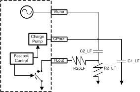
Table 8. Normal Operation vs. Fastlock
| PARAMETER | NORMAL OPERATION | FASTLOCK |
|---|---|---|
| Charge Pump Gain | CPG | FL_CPG |
| FLout Pin | High Impedance | Grounded |
Once the loop filter values and charge pump gain are known for normal operation, they can be determined for Fastlock operation as well. In normal operation, one can not use the highest charge pump gain and still use Fastlock because there will be no larger current to switch in. The resistor and the charge pump current are changed simultaneously so that the phase margin remains the same while the loop bandwidth is multiplied by a factor of K as shown in Table 9:
Table 9. Fastlock Configuration
| PARAMETER | SYMBOL | CALCULATION |
|---|---|---|
| Charge Pump Gain in Fastlock | FL_CPG | Typically use the highest value. |
| Loop Bandwidth Multiplier | K | K=sqrt(FL_CPG/CPG) |
| External Resistor | R2pLF | R2 / (K-1) |
8.3.13 Lock Detect
The LMX2581 offers two circuits to detect lock, Vtune and Digital Lock Detect, which may be used separately or in conjunction. Digital Lock Detect gives a reliable indication of lock/unlock if programmed correctly with the one exception, which occurs when the PLL is locked to a valid OSCin signal and then the OSCin signal is abruptly removed. In this case, digital lock detect can sometimes still indicate a locked state, but Vtune Lock detect will correctly indicate an unlocked state. Therefore, for the most reliable lock detect, it is recommended to use these in conjunction, because each technique's drawback is covered by the other one. Note that because the powerdown mode powers down the lock detect circuitry, it is possible to get a high lock detect indication when the device is powered down. The details of the two respective methods are described below in the Vtune Lock Detect and Digital Lock Detect (DLD) sections.
8.3.13.1 Vtune Lock Detect
This style of lock detect only works with the internal VCO. Whenever the tuning voltage goes below the threshold of about 0.5 V, or above the threshold of about 2.2 V, the internal VCO will become unlocked and the Vtune lock detect will indicate that the device is unlocked. For this reason, when the Vtune lock detect says the PLL is unlocked, one can be certain that it is unlocked.
8.3.13.2 Digital Lock Detect (DLD)
This lock detect works by comparing the phase error as presented to the phase detector. If the phase error plus the delay as specified by the PFD_DLY word outside the tolerance as specified by DLD_TOL, then this comparison would be considered to be an error, otherwise passing. At higher phase detector frequencies, it may be necessary to adjust the DLD_ERR_CNT and DLD_PASS_CNT. The DLD_ERR_CNT specifies how may errors are necessary to cause the circuit to consider the PLL to be unlocked. The DLD_PASS_CNT multiplied by 8 specifies how many passing comparisons are necessary to cause the PLL to be considered to be locked and also resets the count for the errors. The DLD_ERR_CNT and DLD_PASS_CNT values may be decreased to make the circuit more sensitive, but if lock detect is made too sensitive, chattering can occur and these values should be increased.
8.3.14 Part ID and Register Readback
8.3.14.1 Uses of Readback
The LMX2581 allows any of its registers to be read back, which could be useful for the following applications below.
- Register Readback
- By reading back the register values, it can be confirmed that the correct information was written. In addition to this, Register R6 has special diagnostic information that could potentially be useful for debugging problems.
- Part ID Readback
- By reading back the part ID, this information may be used by whatever device is programming the LMX2581 to identify this device and know what programming information to send. In addition to this, the BUFEN and CE pins may be used to create 4 unique part ID values. Although these pins can impact the device, they may be overridden in software. It is not necessary to have the device programmed in order to do part ID Readback.
The procedure for doing this Readback is in the Serial Data Readback Timing section. Depending on the settings for the ID(R0[31]) and RDADDR (R6[8:5]), information a different bit stream will be returned as shown in Table 10.
Table 10. Uses of Readback
| ID | BUFEN PIN | CE PIN | READBACK CODE |
|---|---|---|---|
| 0 | X | X | Readback register defined by RDADDR. |
| 1 | 0 | 0 | 0x 00000500 |
| 0 | 1 | 0x 00000510 | |
| 1 | 0 | 0x 00000520 | |
| 1 | 1 | 0x 00000530 |
8.3.14.2 Serial Timing for Readback
Readback is done through the the MUXout (or LD) pin with the same clock that is used to clock in the data.
- Choose either the MUXout (or LD) pin for reading back data and program the MUXOUT_SELECT (or LD_SELECT) to readback mode.
- Bring the LE pin from low to high to start the readback at the MSB.
- After the signal to the CLK pin goes high, the data will be ready at the readback pin 10 ns afterwards. It is recommended to read back the data on the falling edge of the clock. Technically, the first bit actually becomes ready after the rising edge of LE, but it still needs to be clocked out.
- The address being clocked out will all be 1's.
Because the CLK pin is both used to clock in data and clock out data, special care needs to be taken to ensure that erroneous data is not being clocked in during readback. There are two approaches to deal with this. The first approach is to actually send valid data during readback. For this approach, R6 is a recommended register and the approach is shown in Figure 18:
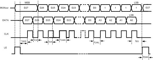 Figure 18. Timing for Readback
A second approach is to hold LE high during readback so that the clock pulses do not clock data into the part, but still function for readback purposes. Figure 19 demonstrates this method:
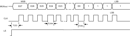 Figure 19. Timing for Readback, Holding LE High
8.3.15 Optimization of Spurs
The LMX2581 offers several programmable features for optimizing fractional spurs. In order to get the best out of these features, it makes sense to understand the different kinds of spurs as well as their behaviors, causes, and remedies. Although optimizing spurs may involve some trial and error, there are ways to make this process more systematic. Texas Instruments offers tools for information and tools for fractional spurs such as Application Note AN-1879 (SNAA062), the Clock Design Tool, and this datasheet.
8.3.15.1 Phase Detector Spur
The phase detector spur occurs at an offset from the carrier equal to the phase detector frequency, fPD. To minimize this spur, considering using a smaller value for PFD_DLY, smaller value for CPG_BLEED, and a lower phase detector frequency. In some cases where the loop bandwidth is very wide relative to the phase detector frequency, some benefit might be gained from using a narrower loop bandwidth or adding poles to the loop filter, but otherwise the loop filter has minimal impact. Bypassing at the supply pins and board layout can also have an impact on this spur, especially at higher phase detector frequencies.
8.3.15.2 Fractional Spur - Integer Boundary Spur
This spur occurs at an offset equal to the difference between the VCO frequency and the closest integer channel for the VCO. For instance, if the phase detector frequency is 100 MHz and the VCO frequency was 2703 MHz, then the integer boundary spur would be at 3 MHz offset. This spur can be either PLL or VCO dominated. If it is PLL dominated, then the following table shows that decreasing the loop bandwidth and some of the programmable fractional words may impact this spur. If the spur is VCO dominated, then reducing the loop filter will not help, but rather reducing the phase detector and having a good slew rate and signal integrity at the OSCin pin will help. Regardless of whether it is PLL or VCO dominated, the VCO core does impact this spur.
Table 11. Typical Integer Boundary Spur Levels
It is common practice to benchmark a fractional PLL spurs by choosing a worst case VCO frequency and use this as a metric. However, one should be cautions that this is only a metric for the integer boundary spur. For instance, suppose that one was to compare two devices by using an 100 MHz phase detector frequency, tune the VCO to 2000.001 MHz, and measure the integer boundary spur at 1 kHz. If one part was to have better spurs at this frequency, this does not necessarily mean that the spurs would be better at a channel farther from an integer boundary, like 2025.001 MHz.
8.3.15.3 Fractional Spur - Primary Fractional Spurs
These spurs occur at multiples of fPD / PLL_DEN and are not the integer boundary spur. For instance, if the phase detector frequency is 100 MHz and the fraction is 3/100, the primary fractional spurs would be at 1,2,4,5,6,...MHz. These are impacted by the loop filter bandwidth and modulator order. If a small frequency error is acceptable, then a larger equivalent fraction may improve these spurs. For instance, if the fraction is 53/200, expressing this as 530,000 / 2,000, 001. This larger unequivalent fraction pushes the fractional spur energy to much lower frequencies that hopefully is not so critical.
8.3.15.4 Fractional Spur - Sub-Fractional Spurs
These spurs appear at a fraction of fPD / PLL_DEN and depend on modulator order. With the first order modulator, there are no sub-fractional spurs. The second order modulator can produce 1/2 sub-fractional spurs if the denominator is even. A third order modulator can produce sub-fractional spurs at 1/2,1/3, or 1/6 of the offset, depending if it is divisible by 2 or 3. For instance, if the phase detector frequency is 100 MHz and the fraction is 3/100, no sub-fractional spurs for a first order modulator or sub-fractional spurs at multiples of 1.5 MHz for a 2nd or 3rd order modulator would be expected.
Aside from strategically choosing the fractional denominator and using a lower order modulator, another tactic to eliminate these spurs is to use dithering and express the fraction in larger equivalent terms (that is, 1000000/4000000 instead of 1/4). If a small frequency error is acceptable, also consider a larger unequivalent fraction like (1000000,4000000). However, dithering can also add phase noise, so if dithering is used, this needs to be managed with the various levels it has and the PFD_DLY word to get the best possible performance.
8.3.15.5 Summary of Spurs and Mitigation Techniques
Table 12 gives a summary of the spurs discussed so far and techniques to mitigate them.
Table 12. Spurs and Mitigation Techniques
| SPUR TYPE | OFFSET | WAYS to REDUCE | TRADE-OFF | |
|---|---|---|---|---|
| Phase Detector | fPD |
|
Although reducing the phase detector frequency does improve this spur, it also degrades phase noise. | |
| Integer Boundary | fVCO mod fPD |
Methods for PLL Dominated Spurs
|
Reducing the loop bandwidth may degrade the total integrated noise if the bandwidth is too narrow. | |
|
Methods for VCO Dominated Spurs
|
Reducing the phase detector may degrade the phase noise and also reduce the capacitance at the Vtune pin. | |||
| Primary Fractional | fPD / PLL_DEN |
|
Decreasing the loop bandwidth too much may degrade in-band phase noise. Also, larger unequivalent fractions only sometimes work | |
| Sub-Fractional | fPD / PLL_DEN / k k=2,3, or 6 |
|
Dithering and larger fractions may increase phase noise. | |
8.4 Device Functional Modes
8.4.1 Full Synthesizer Mode
In this mode, the internal VCO is enabled. When combined with an external reference and loop filter, this mode provides a complete signal source.
8.4.2 External VCO Mode
The LMX2581 allows the user to use an external VCO by using the Fin pin and selecting the external VCO mode for the MODE word. Because this is software selectable, the user may have a setup that switches between the external and internal VCO. Because the Fin pin is close to the RFoutA and RFoutB pins, some care needs to be taken to minimize board crosstalk when both an external VCO and an output buffer is used. If only one output buffer is required, it is recommended to use the RFoutB output because it is physically farther from the Fin pin and therefore will have less board related crosstalk. When using external VCO with a different characteristic, it may be necessary to change the phase detector polarity (CPP).
8.4.3 Powerdown Modes
The LMX2581 can be powered down either fully or partially with the PWDN_MODE word or the CE pin. The two types of powerdown are in the following table.
Table 13. LMX2581 Powerdown Modes
| POWERDOWN STATE | DESCRIPTION |
|---|---|
| Partial Powerdown | VCO, PLL, and Output buffers are powered down, but the LDOs are kept powered up to reduce the time it takes to power the device back up. |
| Full Powerdown | VCO, PLL, Output Buffers, and LDOs are all powered down. |
When coming out of a full powerdown state, it is necessary to do the initial power-on programming sequence described in later sections. If coming out of a partial powerdown state, it is necessary to do the sequence for switching frequencies after initialization, that is described in later sections.
8.5 Programming
The LMX2581 is programmed using several 32-bit registers. A 32-bit shift register is used as a temporary register to indirectly program the on-chip registers. The shift register consists of a data field and an address field. The last LSB bits, ADDR[3:0], form the address field, which is used to decode the internal register address. The remaining 28 bits form the data field DATA[27:0]. While LE is low, serial data is clocked into the shift register upon the rising edge of clock (data is programmed MSB first). When LE goes high, data is transferred from the data field into the selected register bank.
8.5.1 Serial Data Input Timing
There are several programming considerations (see Figure 20):
- A slew rate of at least 30 V/us is recommended for the CLK, DATA, and LE signals
- The DATA is clocked into a shift register on each rising edge of the CLK signal. On the rising edge of the LE signal, the data is sent from the shift registers to an actual counter.
- The LE pin may be held high after programming and this will cause the LMX2581 to ignore clock pulses.
- The CLK signal should not be high when LE transitions to low.
- When CLK and DATA lines are shared between devices, it is recommended to divide down the voltage to the CLK, DATA, and LE pins closer to the minimum voltage. This provides better noise immunity.
- If the CLK and DATA lines are toggled while the in VCO is in lock. As is sometimes the case when these lines are shared with other parts, the phase noise may be degraded during the time of this programming.
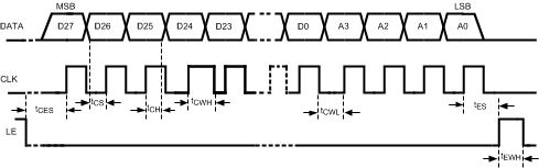 Figure 20. Serial Data Input Timing
8.5.2 Recommended Initial Power on Programming Sequence
When the device is first powered up, the device needs to be initialized and the ordering of this programming is very important. After the following sequence is complete, the device should be running and locked to the proper frequency.
- Apply power to the device and ensure the Vcc pins are at the proper levels.
- Ensure that a valid reference is applied to the OSCin pin
- Program register R5 with RESET (R5[4]) =1
- Program registers R15,R13,R10,R9,R8,R7,R6,R5,R4,R3,R2,R1, and R0
- Wait 20 ms
- Program the R0 register again OR do the recommended sequence for changing frequencies.
8.5.3 Recommended Sequence for Changing Frequencies
The recommended sequence for changing frequencies is as follows:
- (optional) If the OUTx_MUX State is changing, program Register R5
- (optional) If the VCO_DIV state is changing, program Register R3. See VCO_DIV[4:0] — VCO Divider Value if programming a to a value of 4.
- (optional) If the MSB of the fractional numerator or charge pump gain is changing, program register R1
- (Required) Program register R0
Although not necessary, it is also acceptable to program the R0 register a second time after this programming sequence. It is not necessary to program the initial power on sequence to change frequencies.
8.5.4 Triggering Registers
The action of programming certain registers may trigger special actions as shown in Table 14.
Table 14. Triggering Registers
| REGISTER | CONDITIONS | ACTIONS TRIGGERED | WHY THIS IS DONE |
|---|---|---|---|
| R5 | RESET = 1 |
All Registers are reset to power on default values. This takes less than 1 us. The reset bit is self-clearing. |
The registers are reset by the power on reset circuitry when power is initially applied. The RESET bit allows the user the option to perform the same functionality of the power-on reset through software. |
| R0 |
NO_FCAL = 0 |
—Starts the Frequency Calibration —Engages Fastlock (If FL_TOC>0) |
This activates the frequency calibration, which chooses the correct VCO core and also the correct frequency band within that core. This is necessary whenever the frequency is changed. If it is desired that the R0 register be programmed without activating this calibration, then the NO_FCAL bit can be set to zero. If the fastlock timeout counter is programmed to a nonzero value, then this action also engages fastlock. |
| R0 |
NO_FCAL = 1 |
—Engages Fastlock (If FL_TOC>0) | This engages fastlock, which may be used to decrease the lock time in some circumstances. |
8.6 Register Maps
Table 15. Register Map
| Register | 31 | 30 | 29 | 28 | 27 | 26 | 25 | 24 | 23 | 22 | 21 | 20 | 19 | 18 | 17 | 16 | 15 | 14 | 13 | 12 | 11 | 10 | 9 | 8 | 7 | 6 | 5 | 4 | 3 | 2 | 1 | 0 |
|---|---|---|---|---|---|---|---|---|---|---|---|---|---|---|---|---|---|---|---|---|---|---|---|---|---|---|---|---|---|---|---|---|
| DATA[27:0] | ADDRESS[3:0] | |||||||||||||||||||||||||||||||
| R15 | 0 | 0 | 0 | 0 | 0 | 0 | 1 | 0 | 0 | 0 | 0 | 1 | 1 | 1 | 1 | 1 | 1 | 1 | 1 | VCO_ CAP_ MAN |
VCO_CAPCODE[7:0] | 1 | 1 | 1 | 1 | |||||||
| R13 | DLD_ERR_CNT[3:0] | DLD_PASS_CNT[9:0] | DLD_ TOL [2:0] |
1 | 0 | 0 | 0 | 0 | 0 | 1 | 0 | 0 | 0 | 0 | 1 | 1 | 0 | 1 | ||||||||||||||
| R10 | 0 | 0 | 1 | 0 | 0 | 0 | 0 | 1 | 0 | 0 | 0 | 0 | 0 | 0 | 0 | 0 | 0 | 1 | 0 | 1 | 0 | 0 | 0 | 0 | 1 | 1 | 0 | 0 | 1 | 0 | 1 | 0 |
| R9 | 0 | 0 | 0 | 0 | 0 | 0 | 1 | 1 | 1 | 1 | 0 | 0 | 0 | 1 | 1 | 1 | 1 | 1 | 0 | 0 | 0 | 0 | 0 | 0 | 0 | 0 | 1 | 1 | 1 | 0 | 0 | 1 |
| R8 | 0 | 0 | 1 | 0 | 0 | 0 | 0 | 0 | 0 | 1 | 1 | 1 | 1 | 1 | 0 | 1 | 1 | 1 | 0 | 1 | 1 | 0 | 1 | 1 | 1 | 1 | 1 | 1 | 1 | 0 | 0 | 0 |
| R7 | 0 | FL_SELECT [4:0] |
FL_PINMODE [2:0] |
FL_ INV |
MUXOUT_SELECT [4:0] |
MUX_ INV |
MUXOUT_ PINMODE [2:0] |
LD_SELECT [4:0] |
LD_ INV |
LD_ PINMODE[2:0] |
0 | 1 | 1 | 1 | ||||||||||||||||||
| R6 | 0 | RD_DIAGNOSTICS[19:0] | 1 | 0 | RDADDR[3:0] | uWIRE_LOCK | 0 | 1 | 1 | 0 | ||||||||||||||||||||||
| R5 | 0 | 0 | 0 | 0 | 0 | 0 | 0 | OUT _LDEN |
OSC_FREQ[2:0] | BUF EN_ DIS |
0 | 0 | 0 | VCO_ SEL_ MODE [1:0] |
OUTB_ MUX [1:0] |
OUTA _MUX [1:0] |
0_ DLY |
MODE [1:0] |
PWDN_MODE [2:0] |
RESET | 0 | 1 | 0 | 1 | ||||||||
| R4 | PFD_DLY [2:0] |
FL_ FRCE |
FL_TOC[11:0] | FL_CPG[4:0] | 0 | CPG_BLEED[5:0] | 0 | 1 | 0 | 0 | ||||||||||||||||||||||
| R3 | 0 | 0 | 1 | 0 | 0 | 0 | 0 | 0 | 0 | VCO_DIV[4:0] | OUTB_PWR[5:0] | OUTA_PWR[5:0] | OUTB _PD |
OUTA _PD |
0 | 0 | 1 | 1 | ||||||||||||||
| R2 | 0 | 0 | OSC _2X |
0 | CPP | 1 | PLL_DEN[21:0] | 0 | 0 | 1 | 0 | |||||||||||||||||||||
| R1 | CPG[4:0] | VCO_ SEL [1:0] |
PLL_NUM[21:12] | FRAC_ ORDER [2:0] |
PLL_R[7:0] | 0 | 0 | 0 | 1 | |||||||||||||||||||||||
| R0 | ID | FRAC_ DITHER [1:0] |
NO_ FCAL |
PLL_N[11:0] | PLL_NUM[11:0] | 0 | 0 | 0 | 0 | |||||||||||||||||||||||
8.6.1 Programming Word Descriptions
8.6.1.1 Register R15
The programming of register R15 is only necessary when one wants to change the default value of VCO_CAPCODE for improving the VCO calibration time or use the VCO_CAP_MAN bit for diagnostic purposes.
8.6.1.1.1 VCO_CAP_MAN — Manual VCO Band Select
This bit determines if the value of VCO_CAPCODE is just used as a starting point for the initial frequency calibration or if the VCO is forced to this value. If this is forced, it is only for diagnostic purposes.
| VCO_CAP_MAN | IMPACT of VCO_CAPCODE |
|---|---|
| 0 | VCO_CAPCODE value is initial starting point for VCO digital calibration. |
| 1 | VCO_CAPCODE value is forced all the time. For diagnostic purposes only. |
8.6.1.1.2 VCO_CAPCODE[7:0] — Capacitor Value for VCO Band Selection
This word selects the VCO tank capacitor value that is initially used when VCO calibration is run or that is forced when VCO_CAP_MAN is set to one. The lower values correspond to less capacitance, which corresponds to a higher VCO frequency for a given VCO Core. If this word is not programmed, it is defaulted to 128.
| VCO_CAPCODE | VCO TANK CAPACITANCE | VCO FREQUENCY |
|---|---|---|
| 0 | Minimum | Highest |
| ... | ... | ... |
| 255 | Maximum | Lowest |
8.6.1.2 Register R13
Register R13 gives access to words that are used for the digital lock detect circuitry.
8.6.1.2.1 DLD_ERR_CNT[3:0] - Digital Lock Detect Error Count
This is the amount of phase detector comparisons that may exceed the tolerance as specified in DLD_TOL before digital lock indicates an unlocked state. The recommended default is 4 for phase detector frequencies of 80 MHz or below; higher frequencies may require the user to experiment to optimize this value.
8.6.1.2.2 DLD_PASS_CNT[9:0] - Digital Lock Detect Success Count
This value multiplied by 8 is the amount of phase detector comparison within the tolerance specified by DLD_TOL and adjusted by DLD_ERR_CNT that are necessary to cause the digital lock to indicate a locked state. The recommended value is 32 for phase detector frequencies of 80 MHz or below; higher frequencies may require the user to experiment and optimize this value based on application.
8.6.1.2.3 DLD_TOL[2:0] — Digital Lock Detect
This is the tolerance that is used to compare with each phase error to decide if it is a success or a fail. Larger settings are generally recommended, but they are limited by several factors such as PFD_DLY, modulator order, and especially the phase detector frequency.
| DLD_TOL | PHASE ERROR TOLERANCE (ns) | TYPICAL PHASE DETECTOR FREQUENCY |
|---|---|---|
| 0 | 1 | Fpd > 130 MHz |
| 1 | 1.7 | 80 MHz < Fpd ≤ 130 MHz |
| 2 | 3 | 60 MHz < Fpd ≤ 80 MHz |
| 3 | 6 | 45 MHz < Fpd ≤ 60 MHz |
| 4 | 10 | 30 MHz <Fpd ≤ 45 MHz |
| 5 | 18 | Fpd ≤ 30 MHz |
| 6–7 | Reserved | n/a |
8.6.1.3 Registers R10, R9, and R8
These registers control functions that are not disclosed to the user and the power on default values are not optimal. Therefore these registers need to be programmed to the values specified in the register map for proper operation.
8.6.1.4 Register R7
This register has words that control status pins, which would be LD, MUXout, and FLout
8.6.1.4.1 FL_PINMODE[2:0], MUXOUT_PINMODE[2:0], and LD_PINMODE[2:0] — Output Format for Status Pins
These words control the state of the output pin.
| FL_PINMODE MUXOUT_PINMODE LD_PINMODE |
OUTPUT TYPE |
|---|---|
| 0 | TRI-STATE (Default for LD_PINMODE) |
| 1 | Push-Pull (Default for MUXOUT_PINMODE) |
| 2 | Open Drain |
| 3 | High Drive Push-Pull (Can drive 5 mA for an LED) |
| 4 | High Drive Open Drain |
| 5 | High Drive Open Source |
| 6,7 | Reserved |
8.6.1.4.2 FL_INV, MUX_INV, LD_INV - Inversion for Status Pins
The logic for the LD and MUXOUT pins can be inverted with these bits.
| FL_INV MUX_INV LD_INV |
PIN STATUS |
|---|---|
| 0 | Normal Operation |
| 1 | Inverted |
8.6.1.4.3 FL_SELECT[4:0], MUXOUT_SELECT[4:0], LD_SELECT[4:0] — State for Status Pins
This word controls the output state of the MUXout, LD, and FLout pins. Note that during fastlock, the FL_SELECT word is ignored.
| FL_SELECT MUXOUT_SELECT LD_SELECT |
OUTPUT |
|---|---|
| 0 | GND |
| 1 | Digital Lock Detect (Based on Phase Measurement) |
| 2 | Vtune Lock Detect (Based on tuning voltage) |
| 3 | Lock Detect (Based on Phase Measurement AND tuning voltage) |
| 4 | Readback (Default for MUXOUT_SELECT) |
| 5 | PLL_N divided by 2 |
| 6 | PLL_N divided by 4 |
| 7 | PLL_R divided by 2 |
| 8 | PLL_R divided by 4 |
| 9 | Analog Lock Detect |
| 10 | OSCin Detect |
| 11 | Fin Detect |
| 12 | Calibration Running |
| 13 | Tuning Voltage out of Range |
| 14 | VCO calibration fails in the low frequency direction. |
| 15 | VCO Calibration fails in the high frequency direction. |
| 16-31 | Reserved |
8.6.1.5 Register R6
8.6.1.5.1 RD_DIAGNOSTICS[19:0] — Readback Diagnostics
This word is contains several pieces of information that may be read back for debug and diagnostic purposes.
| RD_DIAGNOISTICS[19:8] | |||||||||||
|---|---|---|---|---|---|---|---|---|---|---|---|
| 19 | 18 | 17 | 16 | 15 | [14:11] | 10 | 9 | 8 | |||
| VCO_SELECT | FIN_DETECT | OSCIN_DETECT | VCO_DETECT | Reserved | CAL_ RUNNING |
VCO_RAIL_ HIGH |
VCO_RAIL_ LOW |
||||
| RD_DIAGNOISTICS[7:0] | |||||||||||
|---|---|---|---|---|---|---|---|---|---|---|---|
| 7 | 6 | 5 | 4 | 3 | 2 | 1 | 0 | ||||
| Reserved | VCO_TUNE_ HIGH |
VCO_TUNE_ VALID |
FLOUT_ON | DLD | LD_PIN STATE |
CE_PIN STATE |
BUFEN_PIN STATE |
||||
| WORD NAME | MEANING if VALUE is ONE |
|---|---|
| VCO_ SELECT | This is the VCO that the device chose to use. 0 = VCO 1, 1 = VCO 2, 2 = VCO 3, 3 = VCO 4 |
| FIN_DETECT | Indicates transitions at the Fin pin have been detected. This could either be the VCO signal or self-oscillation of the Fin pin in the even that no signal is present. This bit needs to be manually reset by programing register R5 with R5[30] = 1, and then again with bit R5[30]=0 |
| OSCIN_DETECT | Indicates transitions at the OSCin pin have been detected. This could either be a signal at the OSCin pin or self-oscillation at the OSCin pin in the event no signal is present . This bit needs to be manually reset by programming R5 with R5[29] = 1 and then again with R5[29] = 0. |
| CAL_RUNNING | Indicates that some calibration in the part is currently running. |
| VCO_RAIL_HIGH | Indicates that the VCO frequency calibration failed because the VCO would need to be a higher frequency than it could achieve. |
| VCO_RAIL_LOW | Indicates that the VCO frequency calibration failed because the VCO would need to be a lower frequency than it could achieve. |
| VCO_TUNE_HIGH | Indicates that the VCO tuning voltage is higher than 2.4 volts and outside the allowable range. |
| VCO_TUNE_VALID | Indicates that the VCO tuning voltage is inside then allowable range. |
| FLOUT_ON | Indicates that the FLout pin is low. |
| DLD | Indicates that the digital lock detect phase measurement indicates a locked state. This does not include any consideration of the VCO tuning voltage. |
| LD_PINSTATE | This is the state of the LD Pin. |
| CE_PINSTATE | This is the state of the CE pin. |
| BUFEN_PINSTATE | This is the state of the BUFEN pin. |
8.6.1.5.2 RDADDR[3:0] — Readback Address
When the ID bit is set to zero, this word designates which register is read back from. When the ID bit is set to one, the unique part ID identifying the device as the LMX2581 is read back.
| ID | RDADDR | INFORMATION READ BACK |
|---|---|---|
| 1 | Don't Care | Part ID |
| 0 | 0 | Register R0 |
| 1 | Register R1 | |
| ... | ... | |
| 15 (default) | Register R15 |
8.6.1.5.3 uWIRE_LOCK - Microwire lock
| uWIRE_LOCK | MICROWIRE |
|---|---|
| 0 | Normal Operation |
| 1 | Locked out – All Programming except to the uWIRE_LOCK bit is ignored |
8.6.1.6 Register R5
8.6.1.6.1 OUT_LDEN — Mute Outputs Based on Lock Detect
When this bit is enabled, the RFoutA and RFoutB pins are disabled if the PLL digital lock detect circuitry indicates that the PLL is in the unlocked state.
| OUT_LDEN | PLL DIGITAL LOCK DETECT STATUS | RFoutA / RFoutB PINS |
|---|---|---|
| 0 | Don't Care | Normal Operation |
| 1 | Locked | Normal Operation |
| 1 | Unlocked | Powered Down |
8.6.1.6.2 OSC_FREQ[2:0] — OSCin Frequency for VCO Calibration
This word should be set to in accordance to the OSCin frequency BEFORE the doubler. It is critical for running internal calibrations for this device.
| OSC_FREQ | OSCin FREQUENCY |
|---|---|
| 0 | fOSCin < 64 MHz |
| 1 | 64 ≤ fOSCin < 128 MHz |
| 2 | 128 ≤ fOSCin < 256 MHz |
| 3 | 256 ≤ fOSCin < 512 MHz |
| 4 | 512 ≤ fOSCin |
| ≥ 5 | Reserved |
8.6.1.6.3 BUFEN_DIS - Disable for the BUFEN Pin
This pin allows the BUFEN pin to be disabled. This is useful if one does not want to pull this pin high or use it for the readback ID.
| BUFEN_DIS | BUFEN PIN |
|---|---|
| 0 | Impacts Output buffers |
| 1 | Ignored. |
8.6.1.6.4 VCO_SEL_MODE — Method of Selecting Internal VCO Core
This word allows the user to choose how the VCO selected by the VCO_SEL word is treated. Note setting 0 should not be used if switching from a frequency above 3 GHz to a frequency below 2.2 GHz.
| VCO_SEL_MODE | VCO SELECTION |
|---|---|
| 0 | VCO core is automatically selected based on the last one that was used. If none was used before, it chooses the lowest frequency VCO core. |
| 1 | VCO selection starts at the value as specified by the VCO_SEL word. However, if this is invalid, it will choose another VCO. |
| 2 | VCO is forced to the selection as defined by the VCO_SEL word, regardless of whether it is valid or not. Note that this mode is not ensured and is only included for diagnostic purposes. |
| 3 | Reserved |
8.6.1.6.5 OUTB_MUX — Mux for RFoutB
This word determines whether RFoutB is the VCO frequency, the VCO frequency divided by VCO_DIV, or the fin frequency.
| OUTB_MUX | RFoutB FREQUENCY |
|---|---|
| 0 | fVCO |
| 1 | fVCO / VCO_DIV |
| 2 | fFin |
| 3 | Reserved |
8.6.1.6.6 OUTA_MUX — Mux for RFoutA
This word determines whether RFoutA is the VCO frequency, the VCO frequency divided by VCO_DIV, or the fin frequency.
| OUTA_MUX | RFoutA FREQUENCY |
|---|---|
| 0 | fVCO |
| 1 | fVCO / VCO_DIV |
| 2 | fFin |
| 3 | Reserved |
8.6.1.6.7 0_DLY - Zero Delay Mode
When this mode is enabled, the VCO divider is put in the feedback path of the PLL so that the delay from input to output of the device will be deterministic.
| 0_DLY | PHASE DETECTOR INPUT |
|---|---|
| 0 | Direct VCO or Fin signal. |
| 1 | Channel Divider output. |
8.6.1.6.8 MODE[1:0] — Operating Mode
This word determines in what mode the device is run.
| MODE | OPERATIONAL MODE | PLL | VCO | FIN PIN |
|---|---|---|---|---|
| 0 | Full Chip Mode | Powered Up | Powered Up | Powered Down |
| 1 | PLL Only Mode | Powered Up | Powered Down | Powered Down |
| 2,3 | Reserved | Reserved | Reserved | Reserved |
8.6.1.6.9 PWDN_MODE - Powerdown Mode
This word powers the device up and down. Aside from the traditional power up and power down, there is the partial powerdown that powers down the PLL and VCO, but keeps the LDOs powered up to allow the device to power up faster.
| PWDN_MODE | CE Pin | DEVICE STATUS |
|---|---|---|
| 0 | X | Powered Up |
| 1 | X | Full Powerdown |
| 2 | X | Reserved |
| 3 | X | Partial Powerdown |
| 4 | Low | Full Powerdown |
| High | Powered Up | |
| 5 | X | Reserved |
| 6 | Low | Partial Powerdown |
| High | Powered Up | |
| 7 | Low | Full Powerdown |
| High | Partial Powerdown |
8.6.1.6.10 RESET - Register Reset
When this bit is enabled, the action of programming register R5 resets all registers to their default power on reset status, otherwise the words in register 5 may be programmed without resetting all the registers.
| RESET | ACTION of PROGRAMMING REGISTER R5 |
|---|---|
| 0 | Registers and state machines are operational. |
| 1 | Registers and state machines are reset, then this reset is automatically released. |
8.6.1.7 Register R4
8.6.1.7.1 PFD_DLY[2:0] — Phase Detector Delay
This word controls the minimum on time for the charge pump. The minimum setting often yields the best phase detector spurs and integer mode PLL phase noise. Higher settings may be useful in reducing the delta sigma noise of the modulator when dithering is enabled. These settings are not generally recommended if the phase detector frequency exceeds 130 MHz. If unsure, program this word to zero.
| PFD_DLY | PULSE WIDTH | WHEN RECOMMENDED |
|---|---|---|
| 0 | 370 ps | Default Use with a 2nd order modulator , when dithering is disabled, or when the phase detector frequency is >130 MHz. |
| 1 | 760 ps | Consider these settings for a 3rd order modulator when dithering is used. |
| 2 | 1130 ps | |
| 3 | 1460 ps | |
| 4 | 1770 ps | |
| 5 | 2070 ps | |
| 6 | 2350 ps | |
| 7 | 2600 ps |
8.6.1.7.2 FL_FRCE — Force Fastlock Conditions
This bit forces the fastlock conditions on, provided that the FL_TOC word is greater than zero.
| FL_FRCE | FASTLOCK TIMEOUT COUNTER | FASTLOCK |
|---|---|---|
| 0 | 0 | Disabled |
| > 0 | Fastlock engaged as long as timeout counter is counting down | |
| 1 | 0 | Invalid State |
| > 0 | Always Engaged |
8.6.1.7.3 FL_TOC[11:0] — Fastlock Timeout Counter
This word controls the timeout counter used for fastlock.
| FL_TOC | FASTLOCK TIMEOUT COUNTER | COMMENTS |
|---|---|---|
| 0 | Disabled | Fastlock Disabled |
| 1 | 2 x Reference Cycles | Fastlock engaged as long as timeout counter is counting down |
| 2 | 2 x 2 x Reference cycles | |
| ... | ||
| 4095 | 2 x 4095 x Reference cycles |
8.6.1.7.4 FL_CPG[4:0] — Fastlock Charge Pump Gain
This word determines the charge pump current that is active during fastlock.
| FL_CPG | FASTLOCK CURRENT STATE |
|---|---|
| 0 | TRI-STATE |
| 1 | 1X |
| 2 | 2X |
| .. | ... |
| 31 | 31X |
8.6.1.7.5 CPG_BLEED[5:0]
The CPG bleed word is for advanced users who want to get the lowest possible integer boundary spur. The impact of this word is on the order of 2 dB. For users who do not care about this, the recommendation is to default this word to zero.
| USER TYPE | FRAC_ORDER | CPG | CPG BLEED RECOMMENDATION |
|---|---|---|---|
| Basic User | X | X | 0 |
| Advanced User | < 2 | X | 0 |
| X | < 4X | 0 | |
| >1 | 4X ≤ CPG < 12X | 2 | |
| 12X ≤ CPG | 4 |
8.6.1.8 Register R3
8.6.1.8.1 VCO_DIV[4:0] — VCO Divider Value
This word determines the value of the VCO divider. Note that the this divider may be bypassed with the OUTA_MUX and OUTB_MUX words.
| VCO_DIV | VCO DIVIDER VALUE |
|---|---|
| 0 | 2 |
| 1 | 4 |
| 2 | 6 |
| 3 | 8 |
| 4 | 10 |
| ... | ... |
| 18 | 38 |
| 20 - 31 | Invalid State |
8.6.1.8.2 OUTB_PWR[5:0] — RFoutB Output Power
This word controls the output power for the RFoutB output.
| OUTB_PWR | RFoutB POWER |
|---|---|
| 0 | Minimum |
| ... | ... |
| 47 | Maximum |
| 48 – 63 | Reserved |
8.6.1.8.3 OUTA_PWR[5:0] — RFoutA Output Power
This word controls the output power for the RFoutA output.
| OUTA_PWR | RFout POWER |
|---|---|
| 0 | Minimum |
| ... | ... |
| 47 | Maximum |
| 48 – 63 | Reserved. |
8.6.1.8.4 OUTB_PD — RFoutB Powerdown
This bit powers down the RFoutB output.
| OUTB_PD | RFoutB |
|---|---|
| 0 | Normal Operation |
| 1 | Powered Down |
8.6.1.8.5 OUTA_PD — RFoutA Powerdown
This bit powers down the RFoutA output.
| OUTA_PD | RFoutA |
|---|---|
| 0 | Normal Operation |
| 1 | Powered Down |
8.6.1.9 Register R2
8.6.1.9.1 OSC_2X — OSCin Doubler
This bit controls the doubler for the OSCin frequency.
| OSC_2X | OSCin DOUBLER |
|---|---|
| 0 | Disabled |
| 1 | Enabled |
8.6.1.9.2 CPP - Charge Pump Polarity
This bit sets the charge pump polarity. Note that the internal VCO has a negative tuning gain, so it should be set to negative gain with the internal VCO enabled.
| CPP | CHARGE PUMP POLARITY |
|---|---|
| 0 | Positive |
| 1 | Negative (Default) |
8.6.1.9.3 PLL_DEN[21:0] — PLL Fractional Denominator
These words control the denominator for the PLL fraction. Note that 0 is only permissible in integer mode.
| PLL_ DEN |
PLL_DEN[21:0] | |||||||||||||||||||||
|---|---|---|---|---|---|---|---|---|---|---|---|---|---|---|---|---|---|---|---|---|---|---|
| 0 | 0 | 0 | 0 | 0 | 0 | 0 | 0 | 0 | 0 | 0 | 0 | 0 | 0 | 0 | 0 | 0 | 0 | 0 | 0 | 0 | 0 | 0 |
| 1 | 0 | 0 | 0 | 0 | 0 | 0 | 0 | 0 | 0 | 0 | 0 | 0 | 0 | 0 | 0 | 0 | 0 | 0 | 0 | 0 | 0 | 1 |
| ... | . | . | . | . | . | . | . | . | . | . | . | . | . | . | . | . | . | . | . | . | . | . |
| 4194303 | 1 | 1 | 1 | 1 | 1 | 1 | 1 | 1 | 1 | 1 | 1 | 1 | 1 | 1 | 1 | 1 | 1 | 1 | 1 | 1 | 1 | 1 |
8.6.1.10 Register R1
8.6.1.10.1 CPG[4:0] — PLL Charge Pump Gain
This word determines the charge pump current that used during steady state operation.
| CPG | CHARGE PUMP CURRENT STATE |
|---|---|
| 0 | TRI-STATE |
| 1 | 1X |
| 2 | 2X |
| .. | ... |
| 31 | 31X |
Note that if the CPG setting is 400 µA or lower, then the CPG_BLEED word needs to be set to 0.
8.6.1.10.2 VCO_SEL[1:0] - VCO Selection
These words allow the user to specify which VCO the frequency calibration starts at. If uncertain, program this word to 0 to start at the lowest frequency VCO core. A programming setting of 3 (VCO 4) should not be used if switching to a frequency below 2.2 GHz.
| VCO_SEL | VCO SELECTION |
|---|---|
| 0 | VCO 1 (Lowest Frequency) |
| 1 | VCO 2 |
| 2 | VCO 3 |
| 3 | VCO 4 (Highest Frequency) |
8.6.1.10.3 FRAC_ORDER[2:0] — PLL Delta Sigma Modulator Order
This word sets the order for the fractional engine.
| FRAC_ORDER | MODULATOR ORDER |
|---|---|
| 0 | Integer Mode |
| 1 | 1st Order Modulator |
| 2 | 2nd Order Modulator |
| 3 | 3rd Order Modulator |
| 4-7 | Reserved |
8.6.1.10.4 PLL_R[7:0] — PLL R divider
This word sets the value that divides the OSCin frequency.
| PLL_R | PLL_R DIVIDER VALUE |
|---|---|
| 0 | 256 |
| 1 | 1 (bypass) |
| ... | ... |
| 255 | 255 |
8.6.1.11 Register R0
Register R0 controls the frequency of the device. Also, unless disabled by setting NO_FCAL = 1, the action of writing to the R0 register triggers a frequency calibration for the internal VCO.
8.6.1.11.1 ID - Part ID Readback
When this bit is set, the part ID indicating the device is an LMX2581 is read back from the device. Consult the Feature Description for more details.
| ID | READBACK MODE |
|---|---|
| 0 | Register |
| 1 | Part ID |
8.6.1.11.2 FRAC_DITHER[1:0] — PLL Fractional Dithering
This word sets the dithering mode. When the fractional numerator is zero, it is recommended, although not required, to set the FRAC_DITHER mode to disabled for the best possible spurs. Doing this shuts down the fractional circuitry and eliminates fractional spurs for these frequencies. This is the reason why the FRAC_DITHER word is in the R0 register, so that it can be set correctly for every frequency if this setting changes.
| FRAC_DITHER | DITHERING MODE |
|---|---|
| 0 | Weak |
| 1 | Medium |
| 2 | Strong |
| 3 | Disabled |
8.6.1.11.3 NO_FCAL — Disable Frequency Calibration
Normally, when the R0 register is written to, a frequency calibration for the internal VCO is triggered. However, this feature may be disabled. If the frequency is changed, then this frequency calibration is necessary for the internal VCO.
| NO_FCAL | VCO FREQUENCY CALIBRATION |
|---|---|
| 0 | Done upon write to R0 Register |
| 1 | Not done on write to R0 Register |
8.6.1.11.4 PLL_N - PLL Feedback Divider Value
This is the feedback divider value for the PLL. There are some restrictions on this depending on the modulator order.
| PLL_N | PLL_N[11:0] | |||||||||||
|---|---|---|---|---|---|---|---|---|---|---|---|---|
| <7 | Invalid state | |||||||||||
| 7 | Possible only in integer mode or with a 1st order modulator | |||||||||||
| 8-9 | Possible in integer mode, 1st order modulator, or 2nd order modulator | |||||||||||
| 10-13 | Possible only in integer mode, 1st order modulator, 2nd order modulator, or 3rd order modulator | |||||||||||
| 14 | 0 | 0 | 0 | 0 | 0 | 0 | 0 | 0 | 1 | 1 | 1 | 0 |
| ... | ... | ... | ... | ... | ... | ... | ... | ... | ... | ... | ... | ... |
| 4095 | 1 | 1 | 1 | 1 | 1 | 1 | 1 | 1 | 1 | 1 | 1 | 1 |
8.6.1.11.5 PLL_NUM[21:12] and PLL_NUM[11:0] — PLL Fractional Numerator
These words control the numerator for the PLL fraction.
| PLL_ NUM |
PLL_NUM[21:12] | PLL_NUM[11:0] | ||||||||||||||||||||
|---|---|---|---|---|---|---|---|---|---|---|---|---|---|---|---|---|---|---|---|---|---|---|
| 0 | 0 | 0 | 0 | 0 | 0 | 0 | 0 | 0 | 0 | 0 | 0 | 0 | 0 | 0 | 0 | 0 | 0 | 0 | 0 | 0 | 0 | 0 |
| 1 | 0 | 0 | 0 | 0 | 0 | 0 | 0 | 0 | 0 | 0 | 0 | 0 | 0 | 0 | 0 | 0 | 0 | 0 | 0 | 0 | 0 | 1 |
| ... | . | . | . | . | . | . | . | . | . | . | . | . | . | . | . | . | . | . | . | . | . | . |
| 4095 | 0 | 0 | 0 | 0 | 0 | 0 | 0 | 0 | 0 | 0 | 1 | 1 | 1 | 1 | 1 | 1 | 1 | 1 | 1 | 1 | 1 | 1 |
| 4096 | 0 | 0 | 0 | 0 | 0 | 0 | 0 | 0 | 0 | 1 | 0 | 0 | 0 | 0 | 0 | 0 | 0 | 0 | 0 | 0 | 0 | 0 |
| ... | . | . | . | . | . | . | . | . | . | . | . | . | . | . | . | . | . | . | . | . | . | . |
| 4194303 | 1 | 1 | 1 | 1 | 1 | 1 | 1 | 1 | 1 | 1 | 1 | 1 | 1 | 1 | 1 | 1 | 1 | 1 | 1 | 1 | 1 | 1 |