SNVS641L January   2010  – April 2019 LMZ10503

PRODUCTION DATA.  

  1. Features
  2. Applications
  3. Description
    1.     Device Images
      1.      Typical Application Circuit
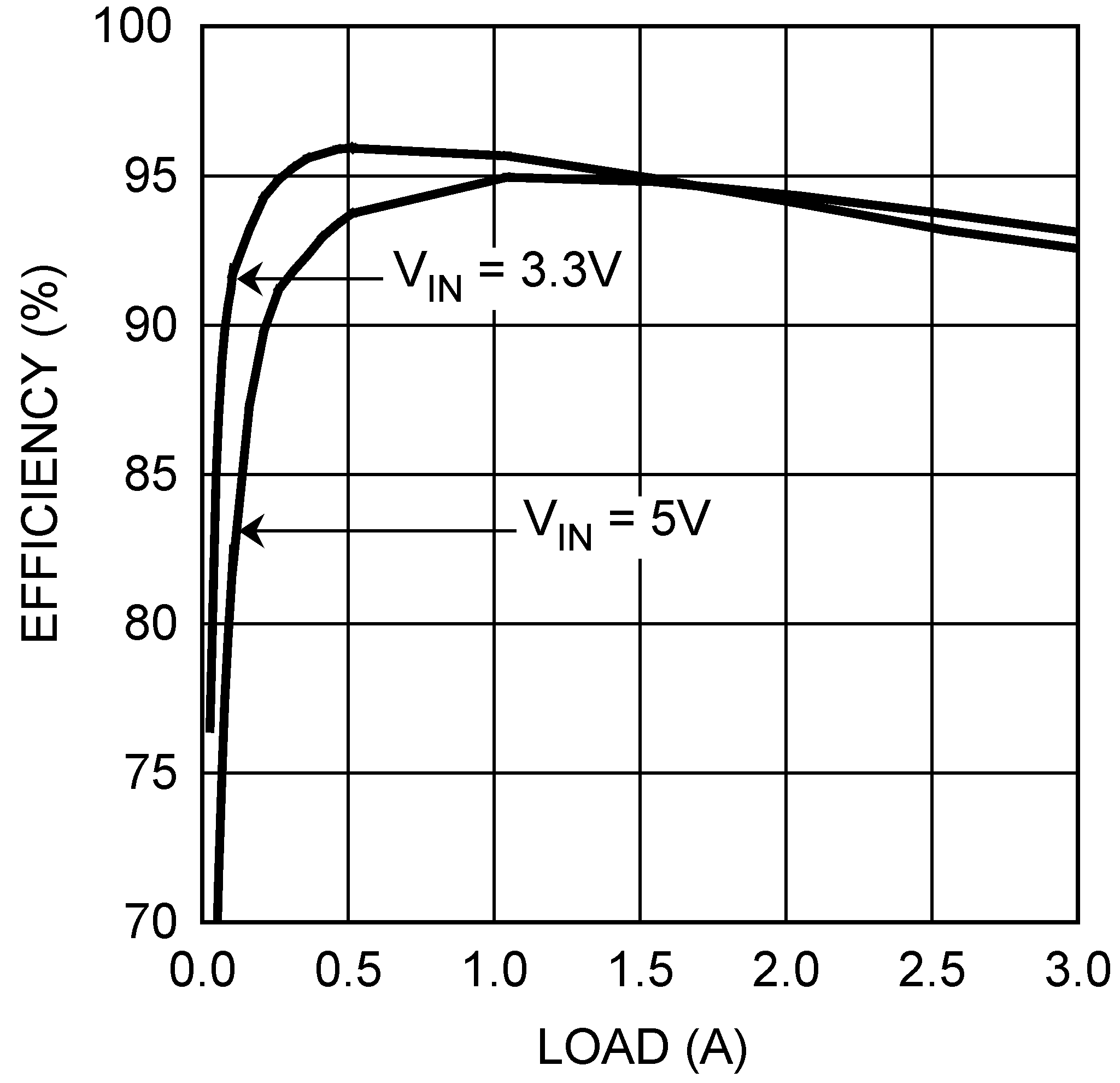
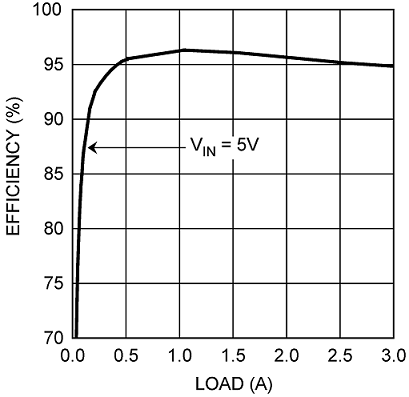
      2.      Efficiency VOUT = 3.3 V
  4. Revision History
  5. Pin Configuration and Functions
    1.     Pin Functions
  6. Specifications
    1. 6.1 Absolute Maximum Ratings
    2. 6.2 ESD Ratings
    3. 6.3 Recommended Operating Conditions
    4. 6.4 Thermal Information
    5. 6.5 Electrical Characteristics
    6. 6.6 Typical Characteristics
  7. Detailed Description
    1. 7.1 Overview
    2. 7.2 Functional Block Diagram
    3. 7.3 Feature Description
      1. 7.3.1 Enable
      2. 7.3.2 Enable and UVLO
      3. 7.3.3 Soft-Start
      4. 7.3.4 Soft-Start Capacitor
      5. 7.3.5 Tracking
      6. 7.3.6 Tracking - Equal Soft-Start Time
      7. 7.3.7 Tracking - Equal Slew Rates
      8. 7.3.8 Current Limit
      9. 7.3.9 Overtemperature Protection
    4. 7.4 Device Functional Modes
      1. 7.4.1 Prebias Start-Up Capability
  8. Application and Implementation
    1. 8.1 Application Information
    2. 8.2 Typical Application
      1. 8.2.1 Design Requirements
      2. 8.2.2 Detailed Design Procedure
        1. 8.2.2.1 Custom Design With WEBENCH® Tools
        2. 8.2.2.2 Input Capacitor Selection
        3. 8.2.2.3 Output Capacitor Selection
          1. 8.2.2.3.1 Output Voltage Setting
        4. 8.2.2.4 Loop Compensation
      3. 8.2.3 Application Curves
    3. 8.3 System Examples
      1. 8.3.1 Application Schematic for 3.3-V to 5-V Input and 2.5-V Output With Optimized Ripple and Transient Response
      2. 8.3.2 Application Schematic for 3.3-V to 5-V Input and 2.5-V Output
      3. 8.3.3 EMI Tested Schematic for 2.5-V Output Based on 3.3-V to 5-V Input
  9. Power Supply Recommendations
  10. 10Layout
    1. 10.1 Layout Guidelines
    2. 10.2 Layout Examples
    3. 10.3 Estimate Power Dissipation and Thermal Considerations
    4. 10.4 Power Module SMT Guidelines
  11. 11Device and Documentation Support
    1. 11.1 Device Support
      1. 11.1.1 Third-Party Products Disclaimer
      2. 11.1.2 Development Support
        1. 11.1.2.1 Custom Design With WEBENCH® Tools
    2. 11.2 Documentation Support
      1. 11.2.1 Related Documentation
    3. 11.3 Receiving Notification of Documentation Updates
    4. 11.4 Community Resources
    5. 11.5 Trademarks
    6. 11.6 Electrostatic Discharge Caution
    7. 11.7 Glossary
  12. 12Mechanical, Packaging, and Orderable Information

Package Options

Mechanical Data (Package|Pins)
Thermal pad, mechanical data (Package|Pins)
Orderable Information

Typical Characteristics

Unless otherwise specified, the following conditions apply: VIN = VEN = 5 V, CIN is 47 µF 10-V X5R ceramic capacitor; TA = 25°C for efficiency curves and waveforms.
LMZ10503 30111871.png
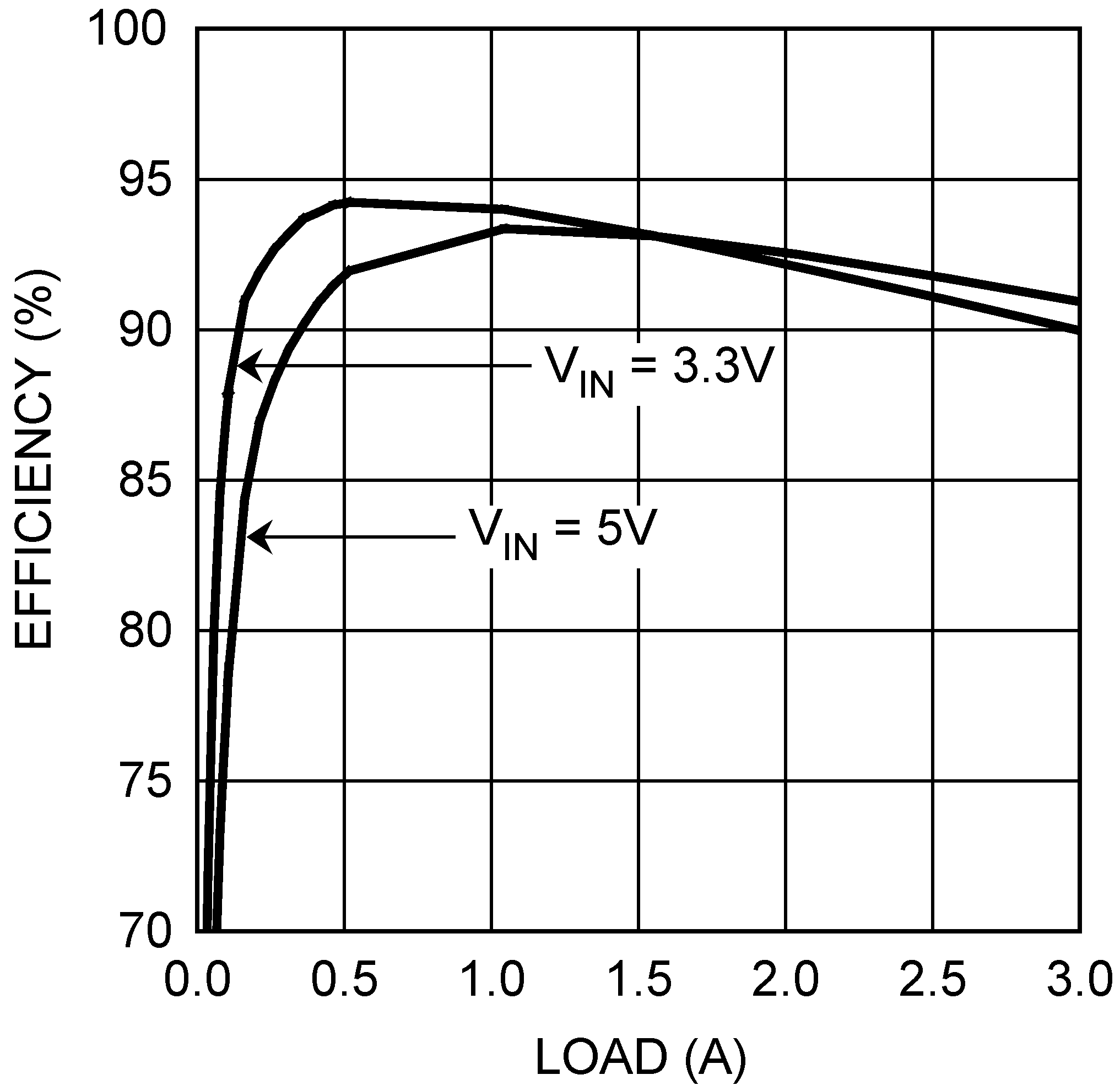
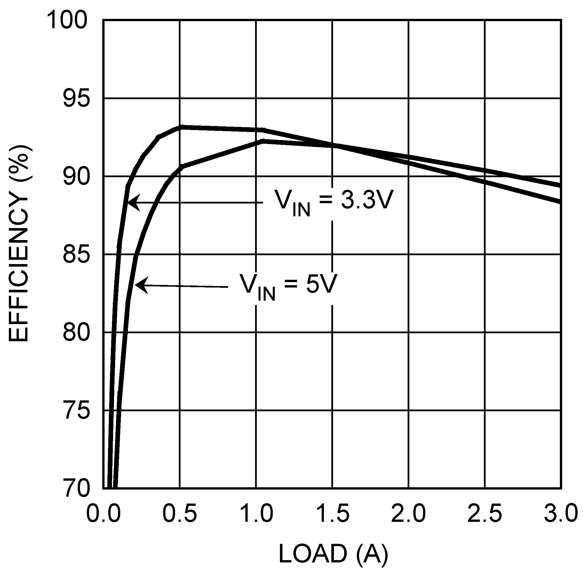
VOUT = 3.3 V
Figure 1. Efficiency
LMZ10503 30111869.png
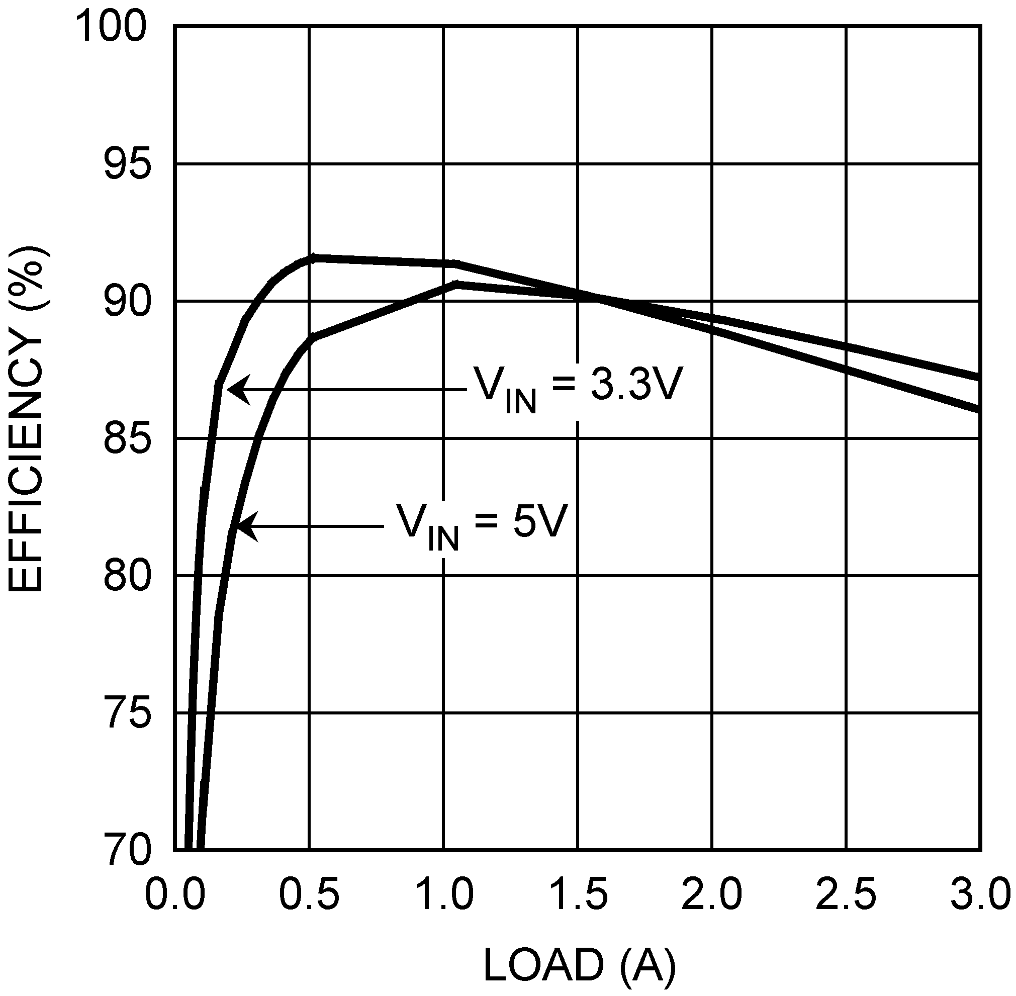
VOUT = 1.8 V
Figure 3. Efficiency
LMZ10503 30111868.png
VOUT = 1.2 V
Figure 5. Efficiency
LMZ10503 301118b3.png
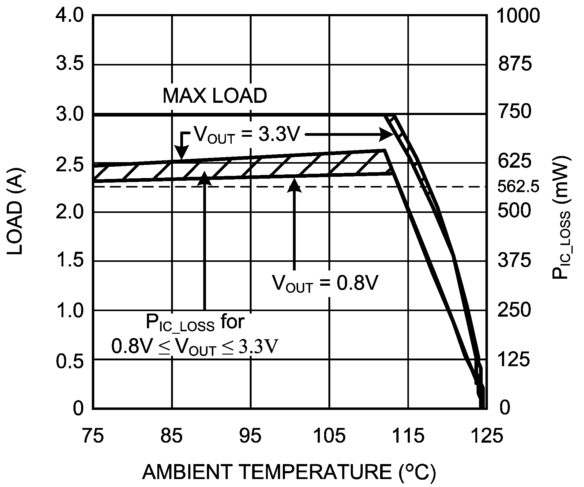
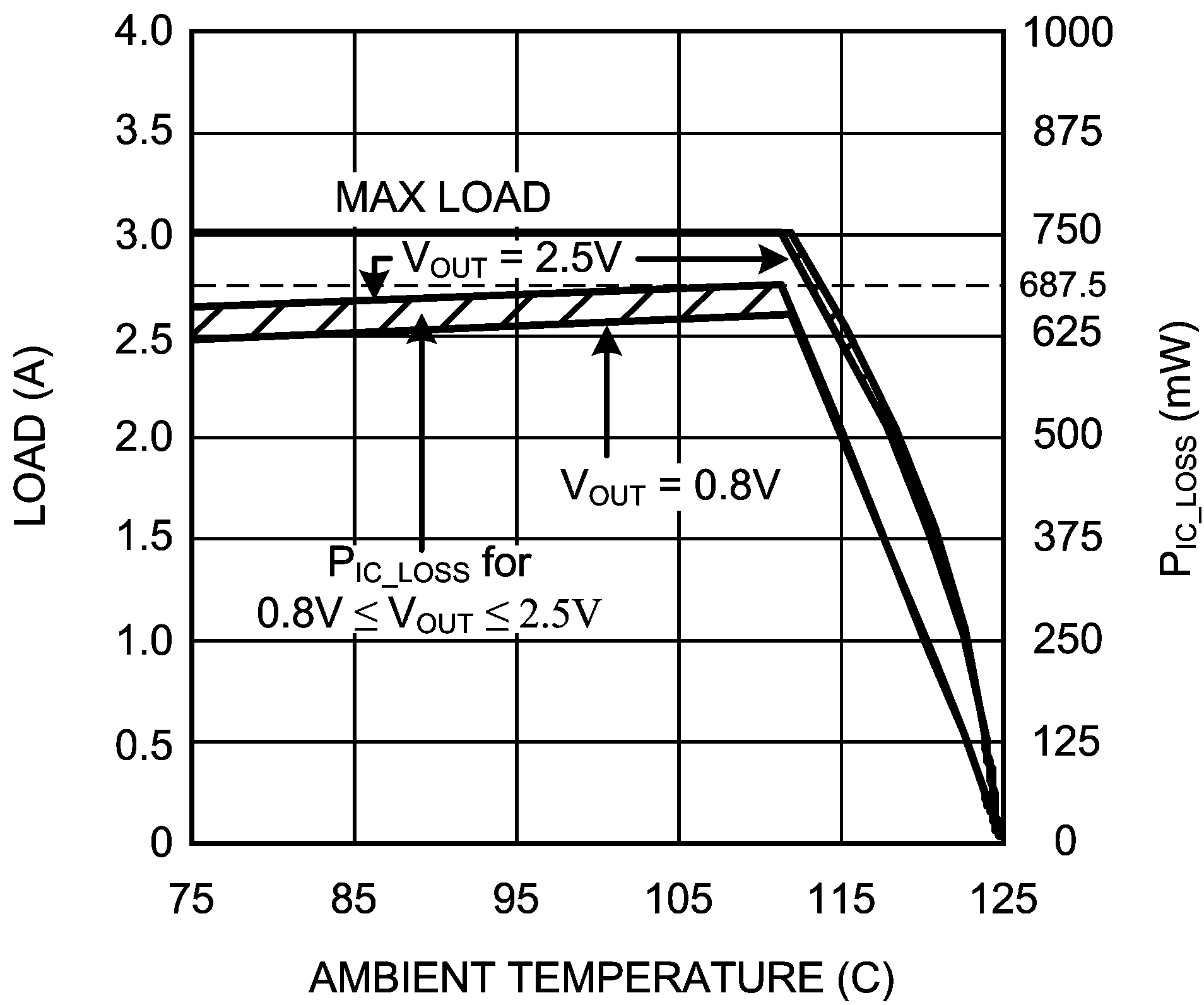
VIN = 5 V, RθJA = 20°C/W
Figure 7. Current Derating
LMZ10503 301118a6.png
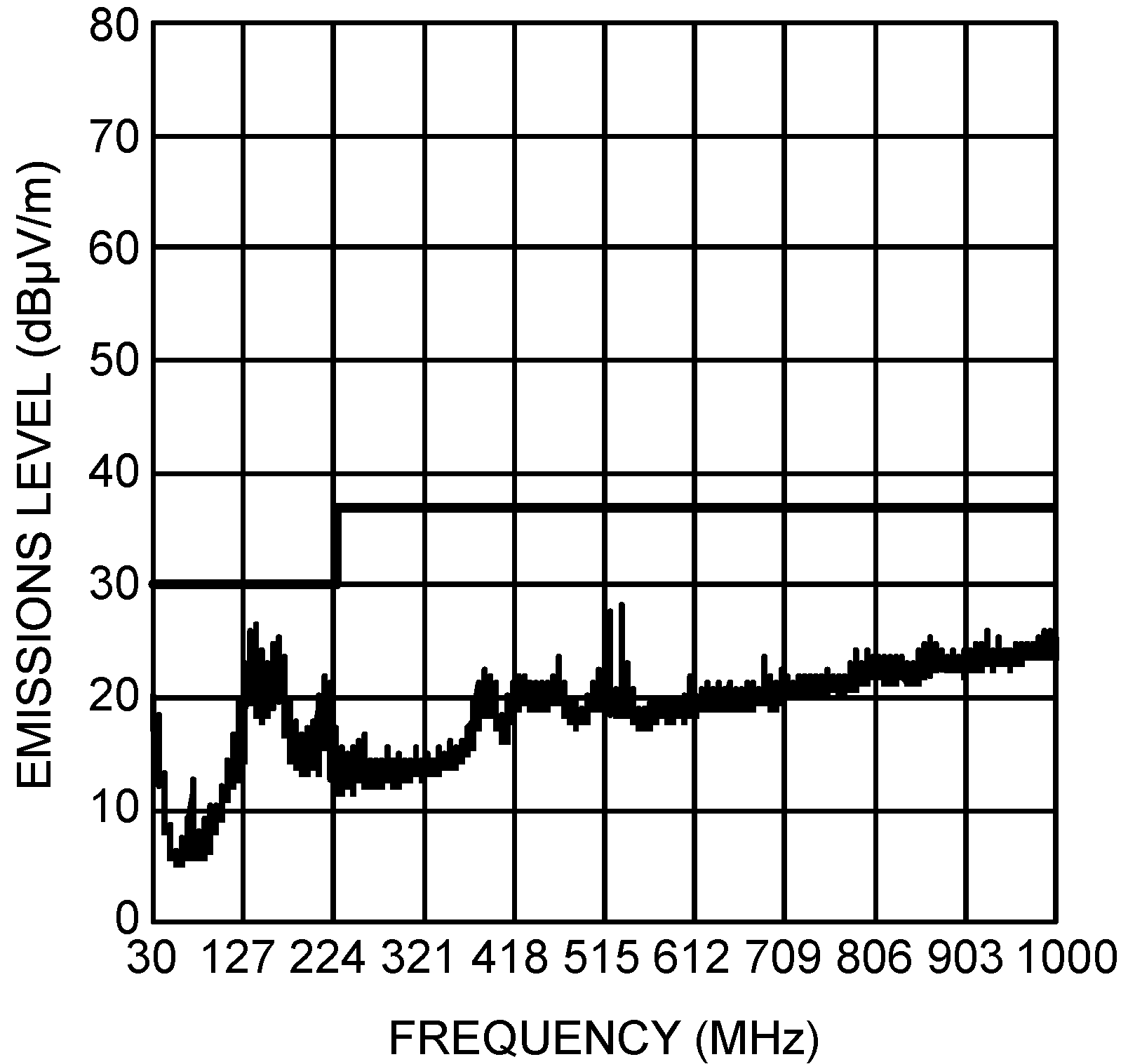
VIN = 5 V, VOUT = 2.5 V, IOUT = 3 A
Figure 9. Radiated Emissions (EN55022, Class B)
Evaluation Board
LMZ10503 30111855.png
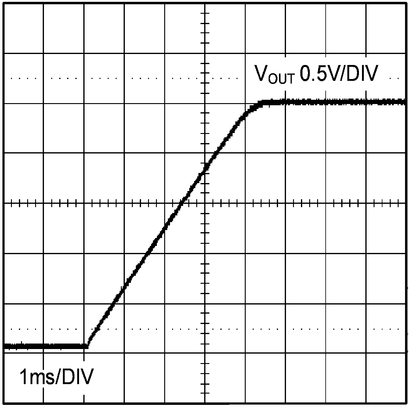
VOUT = 2.5 V, IOUT = 0 A
Figure 11. Prebiased Start-Up
LMZ10503 30111863.png
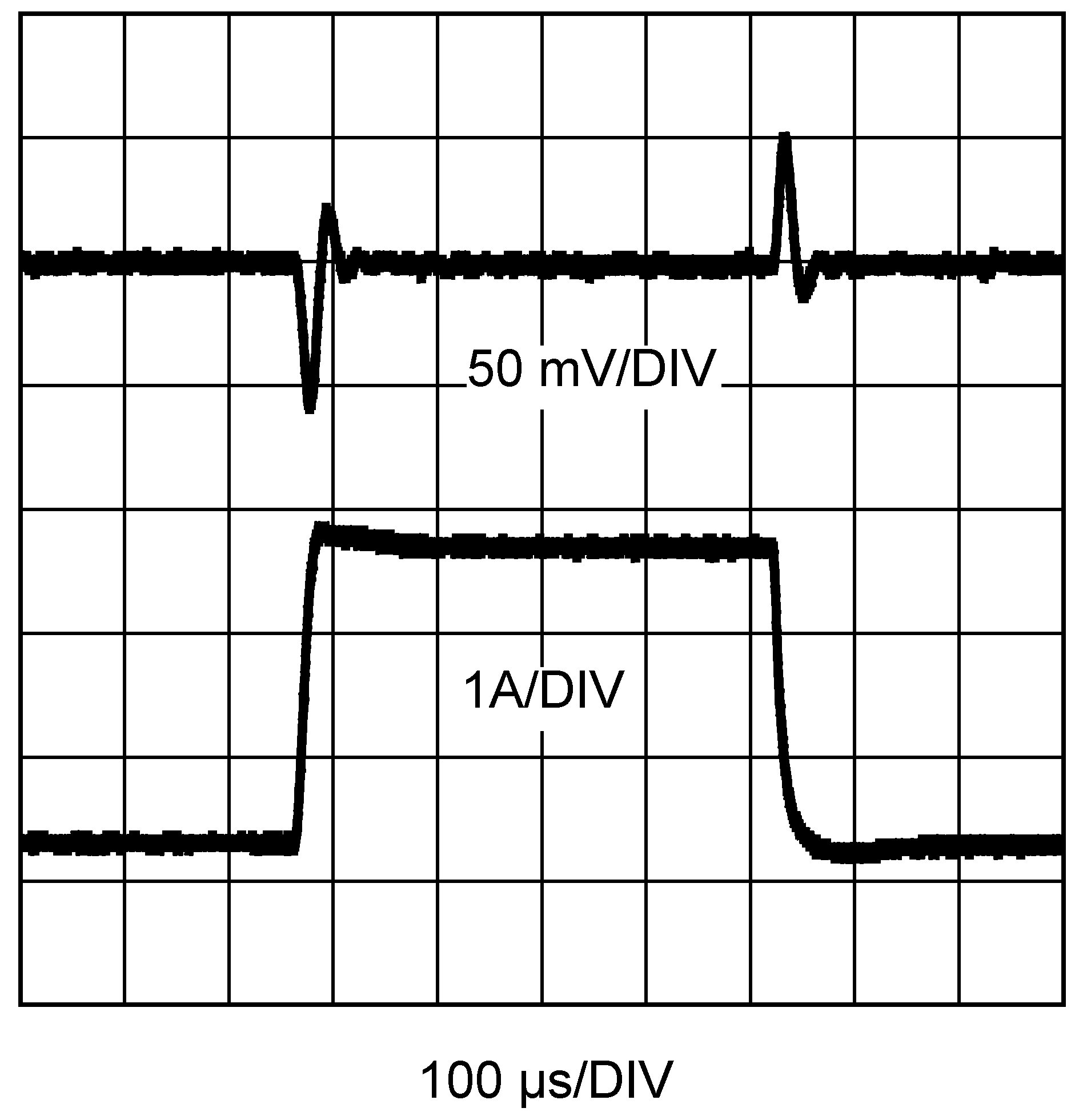
VIN = 5 V, VOUT = 2.5 V, IOUT = 0.3 A to 2.7 A to 0.3-A step
20-MHz Bandwidth Limited. Refer to Table 5 for BOM, includes optional components
Figure 13. Load Transient Response
LMZ10503 30111865.png
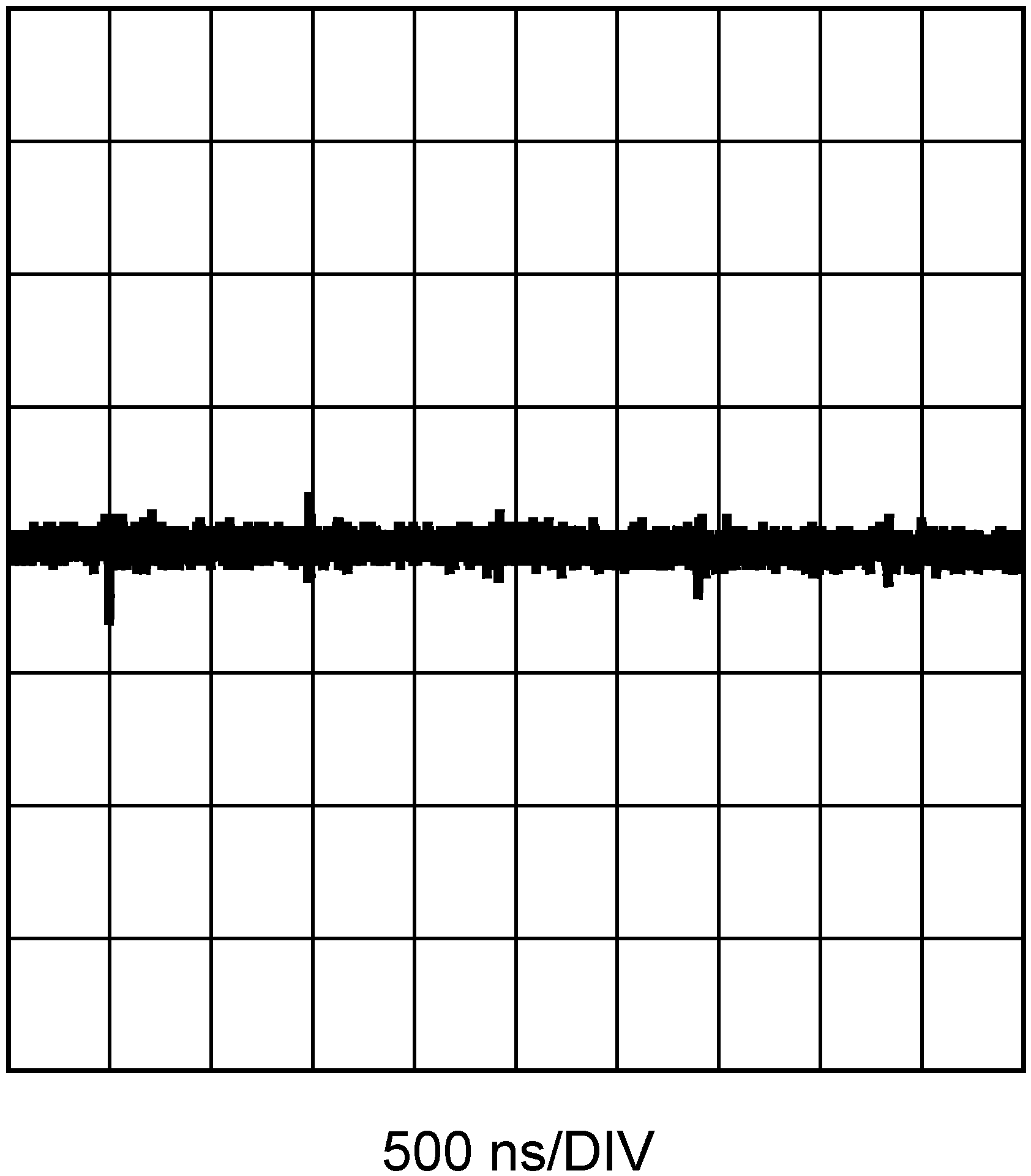
VIN = 5 V, VOUT = 2.5 V, IOUT = 3 A,
20 mV/DIV. Refer to Table 5 for BOM
Figure 15. Output Voltage Ripple
LMZ10503 30111870.png
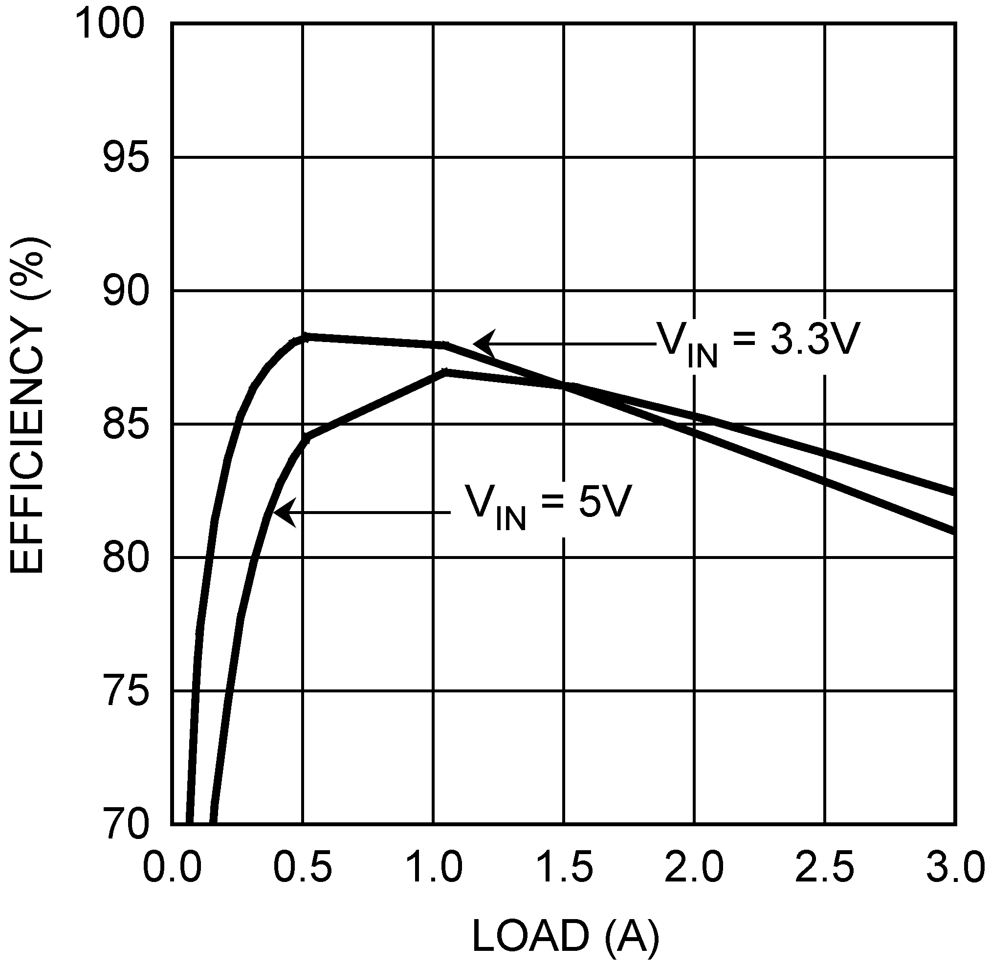
VOUT = 2.5 V
Figure 2. Efficiency
LMZ10503 301118a0.png
VOUT = 1.5 V
Figure 4. Efficiency
LMZ10503 30111867.png
VOUT = 0.8 V
Figure 6. Efficiency
LMZ10503 301118b4.png
VIN = 3.3 V, RθJA = 20°C/W
Figure 8. Current Derating
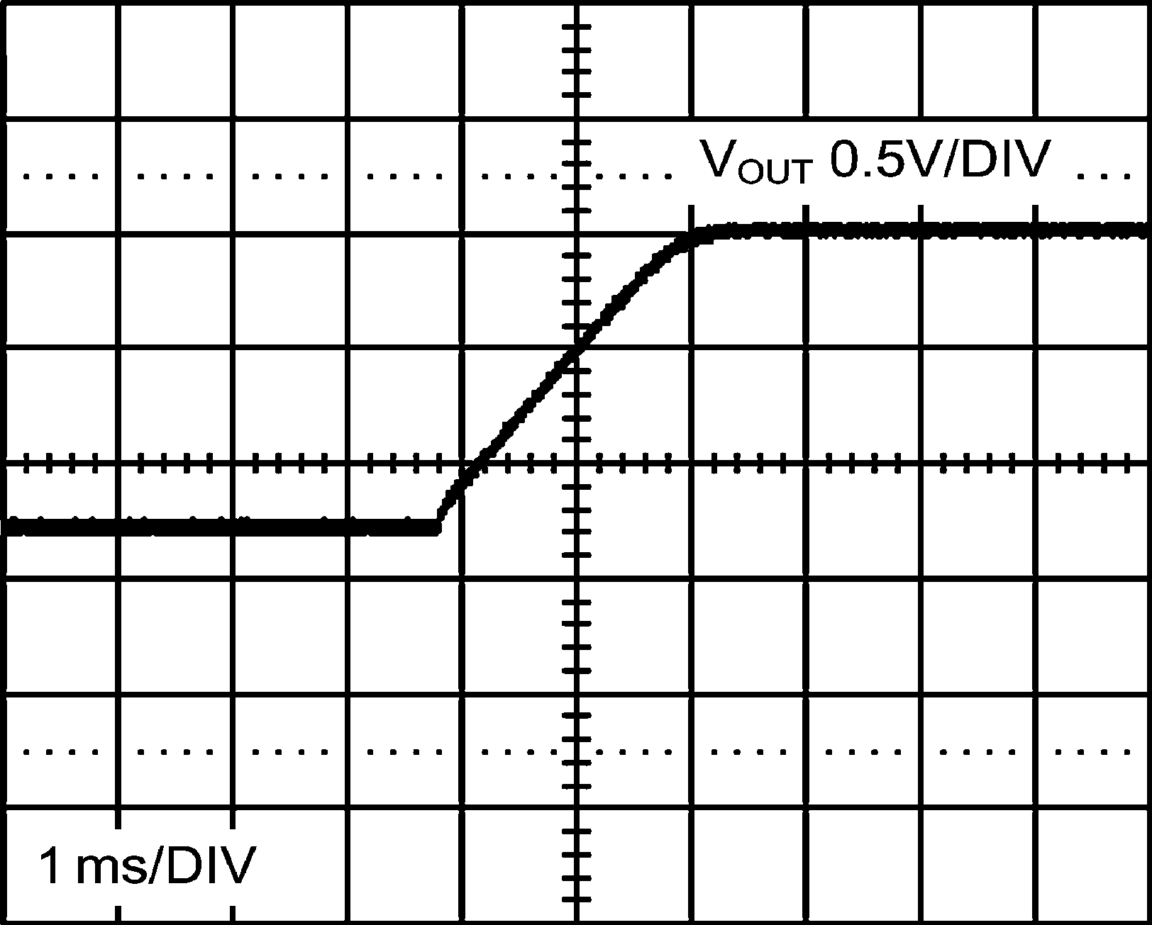
LMZ10503 30111856.png
VOUT = 2.5 V, IOUT = 0 A
Figure 10. Start-Up
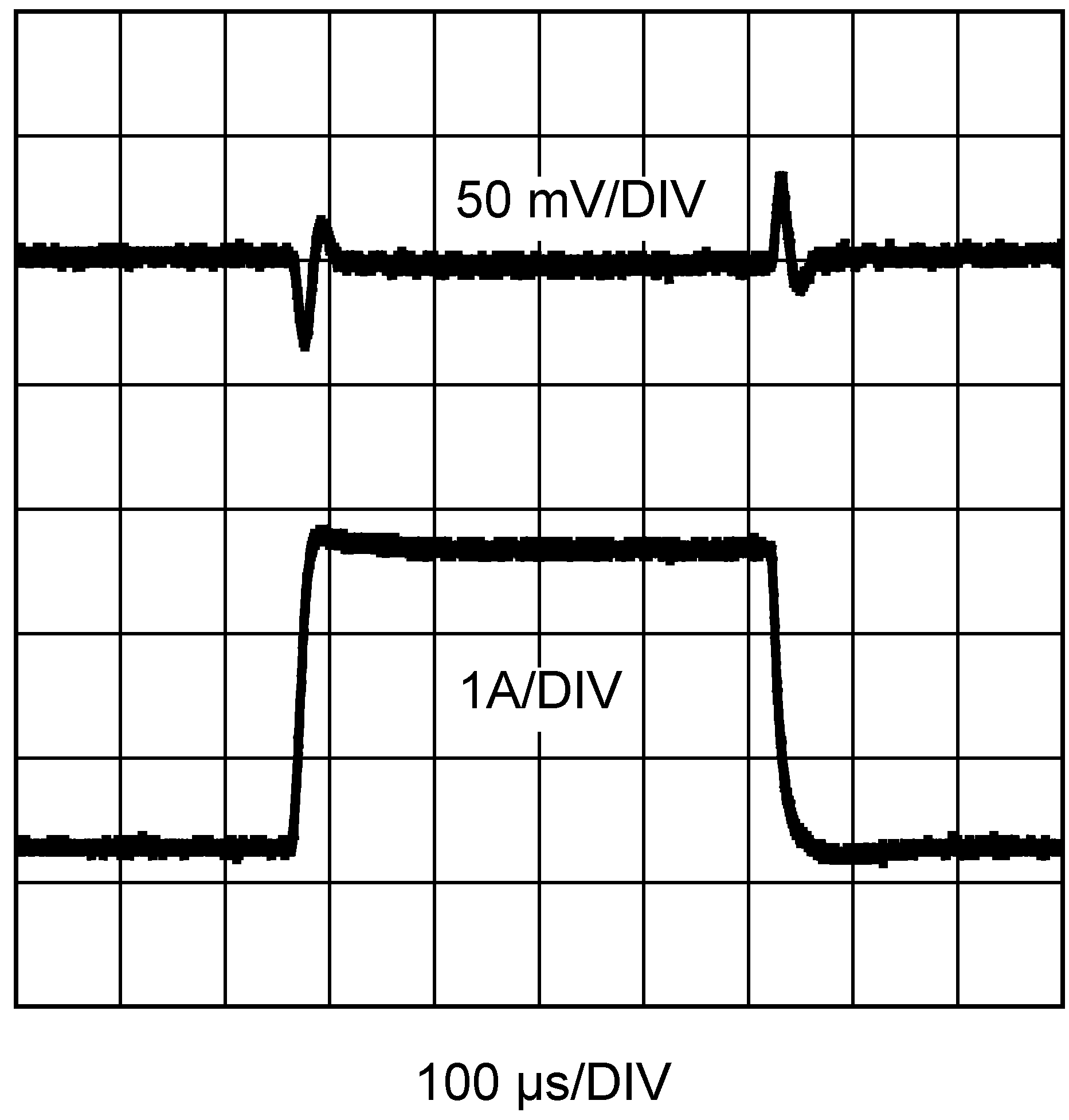
LMZ10503 30111862.png
VIN = 3.3 V, VOUT = 2.5 V, IOUT = 0.3 A to 2.7 A to 0.3-A Step
20-MHz Bandwidth Limited. Refer to Table 5 for BOM, includes optional components
Figure 12. Load Transient Response
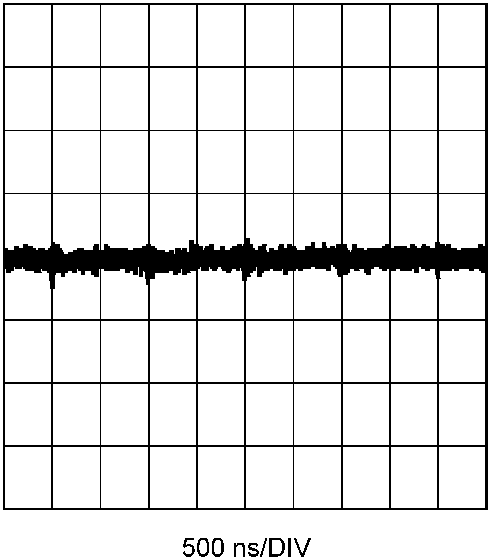
LMZ10503 30111864.png
VIN = 3.3 V, VOUT = 2.5 V, IOUT = 3 A,
20 mV/DIV. Refer to Table 5 for BOM
Figure 14. Output Voltage Ripple