SNVS716H March 2011 – February 2016 LMZ12008
PRODUCTION DATA.
- 1 Features
- 2 Applications
- 3 Description
- 4 Revision History
- 5 Pin Configuration and Functions
- 6 Specification
- 7 Detailed Description
- 8 Application and Implementation
- 9 Power Supply Recommendations
- 10Layout
- 11Device and Documentation Support
- 12Mechanical, Packaging, and Orderable Information
Package Options
Mechanical Data (Package|Pins)
- NDY|11
Thermal pad, mechanical data (Package|Pins)
Orderable Information
6 Specification
6.1 Absolute Maximum Ratings (1)(2)(3)
| MIN | MAX | UNIT | |
|---|---|---|---|
| VIN to PGND | –0.3 | 24 | V |
| EN to AGND | –0.3 | 5.5 | V |
| SS, FB to AGND | –0.3 | 2.5 | V |
| AGND to PGND | –0.3 | 0.3 | V |
| Junction Temperature | 150 | °C | |
| Peak Reflow Case Temperature (30 sec) | 245 | °C | |
| Storage Temperature, Tstg | –65 | 150 | °C |
(1) Stresses beyond those listed under Absolute Maximum Ratings may cause permanent damage to the device. These are stress ratings only, which do not imply functional operation of the device at these or any other conditions beyond those indicated under Recommended Operating Conditions. Exposure to absolute-maximum-rated conditions for extended periods may affect device reliability.
(2) If Military/Aerospace specified devices are required, please contact the Texas Instruments Sales Office/ Distributors for availability and specifications.
(3) For soldering specifications, refer to the following document: SNOA549
6.2 ESD Ratings
| VALUE | UNIT | |||
|---|---|---|---|---|
| V(ESD) | Electrostatic discharge | Human body model (HBM), per ANSI/ESDA/JEDEC JS-001(1) | ±2000 | V |
(1) JEDEC document JEP155 states that 500-V HBM allows safe manufacturing with a standard ESD control process.
6.3 Recommended Operating Conditions(1)
| MIN | MAX | UNIT | |
|---|---|---|---|
| VIN | 6 | 20 | V |
| EN | 0 | 5 | V |
| Operation Junction Temperature | −40 | 125 | °C |
(1) Absolute Maximum Ratings are limits beyond which damage to the device may occur. Operating Ratings are conditions under which operation of the device is intended to be functional. For ensured specifications and test conditions, see the Electrical Characteristics.
6.4 Thermal Information
| THERMAL METRIC(1) | LMZ12008 | UNIT | ||
|---|---|---|---|---|
| NDY | ||||
| 11 PINS | ||||
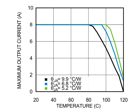
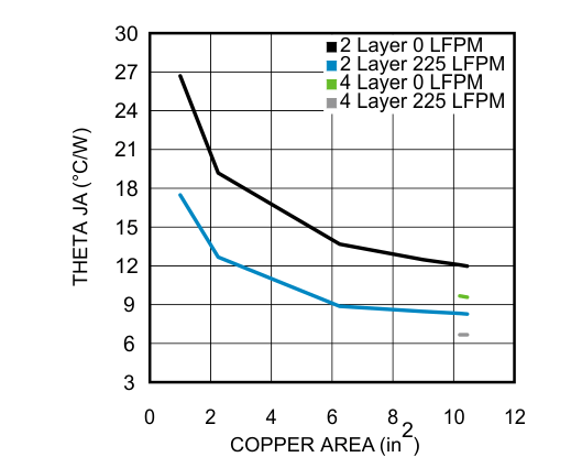
| RθJA | Junction-to-ambient thermal resistance | Natural Convection | 9.9 | °C/W |
| 225 LFPM | 6.8 | |||
| 500 LFPM | 5.2 | |||
| RθJC(top) | Junction-to-case (top) thermal resistance | 1.0 | °C/W | |
(1) For more information about traditional and new thermal metrics, see the Semiconductor and IC Package Thermal Metrics application report, SPRA953.
6.5 Electrical Characteristics
Limits are for TJ = 25°C unless otherwise specified. Minimum and Maximum limits are ensured through test, design or statistical correlation. Typical values represent the most likely parametric norm at TJ = 25°C, and are provided for reference purposes only. Unless otherwise stated the following conditions apply: VIN = 12V, VOUT = 3.3V(1)| PARAMETER | TEST CONDITIONS | MIN(2) | TYP(3) | MAX(2) | UNIT | ||
|---|---|---|---|---|---|---|---|
| SYSTEM PARAMETERS | |||||||
| ENABLE CONTROL | |||||||
| VEN | EN threshold | VEN rising | 1.274 | V | |||
| over the junction temperature (TJ) range of –40°C to +125°C | 1.096 | 1.452 | |||||
| IEN-HYS | EN hysteresis source current | VEN > 1.274 V | 13 | µA | |||
| SOFT-START | |||||||
| ISS | SS source current | VSS = 0 V | 50 | µA | |||
| over the junction temperature (TJ) range of –40°C to +125°C | 40 | 60 | |||||
| tSS | Internal soft-start interval | 1.6 | msec | ||||
| CURRENT LIMIT | |||||||
| ICL | Current limit threshold | DC average | 10.5 | A | |||
| INTERNAL SWITCHING OSCILLATOR | |||||||
| fosc | Free-running oscillator frequency | 314 | 359 | 404 | kHz | ||
| REGULATION AND OVERVOLTAGE COMPARATOR | |||||||
| VFB | In-regulation feedback voltage | VSS >+ 0.8 V IO = 8 A |
0.795 | V | |||
| over the junction temperature (TJ) range of –40°C to +125°C | 0.775 | 0.815 | |||||
| VFB-OV | Feedback overvoltage protection threshold | 0.86 | V | ||||
| IFB | Feedback input bias current | 5 | nA | ||||
| IQ | Non-Switching Quiescent Current | 3 | mA | ||||
| ISD | Shutdown Quiescent Current | VEN = 0 V | 32 | μA | |||
| Dmax | Maximum Duty Factor | 85% | |||||
| THERMAL CHARACTERISTICS | |||||||
| TSD | Thermal Shutdown | Rising | 165 | °C | |||
| TSD-HYST | Thermal shutdown hysteresis | Falling | 15 | °C | |||
| PERFORMANCE PARAMETERS(4) | |||||||
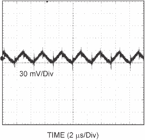
| ΔVO | Output voltage ripple | BW at 20 MHz | 24 | mVPP | |||
| ΔVO/ΔVIN | Line regulation | VIN = 12 V to 20 V, IOUT= 8 A | ±0.2% | ||||
| ΔVO/ΔIOUT | Load regulation | VIN = 12 V, IOUT= 0.001 A to 8 A | 1 | mV/A | |||
| η | Peak efficiency | VIN = 12 V VOUT = 3.3 V, IOUT = 5 A | 89.5% | ||||
| η | Full load efficiency | VIN = 12 V VOUT = 3.3 V, IOUT = 8 A | 88.5% | ||||
(1) EN 55022:2006, +A1:2007, FCC Part 15 Subpart B, tested on Evaluation Board with EMI configuration
(2) Min and Max limits are 100% production tested at 25°C. Limits over the operating temperature range are ensured through correlation using Statistical Quality Control (SQC) methods. Limits are used to calculate Average Outgoing Quality Level (AOQL).
(3) Typical numbers are at 25°C and represent the most likely parametric norm.
(4) Refer to BOM in Table 1.
6.6 Typical Characteristics
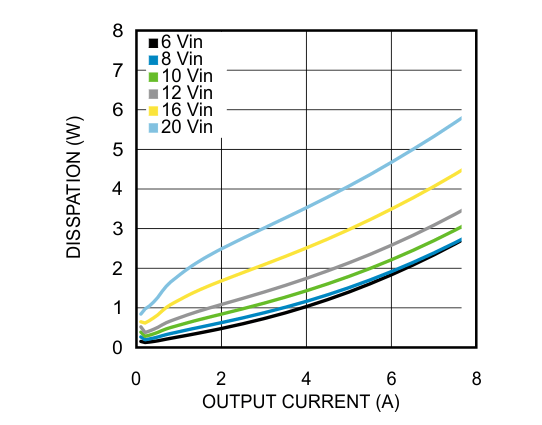
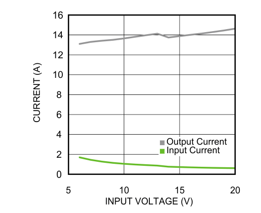
Unless otherwise specified, the following conditions apply: VIN = 12 V; CIN = three × 10 μF + 47-nF X7R Ceramic; COUT = two × 330-μF Specialty Polymer + 47-µF Ceramic + 47-nF Ceramic; CFF = 4.7 nF; TA = 25° C for waveforms. All indicated temperatures are ambient.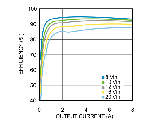
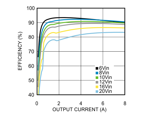
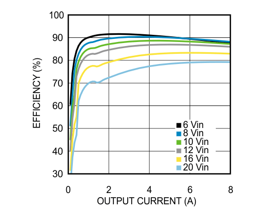
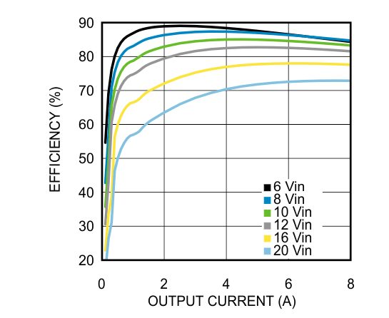
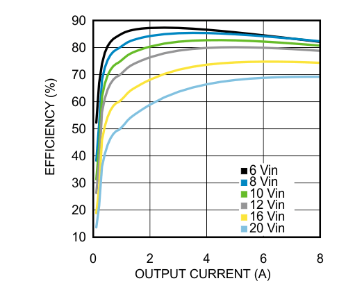
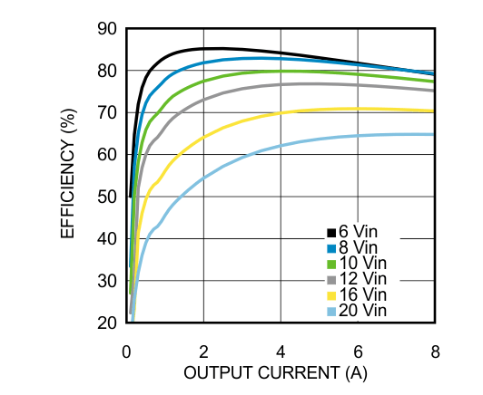
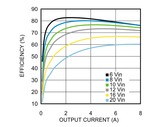
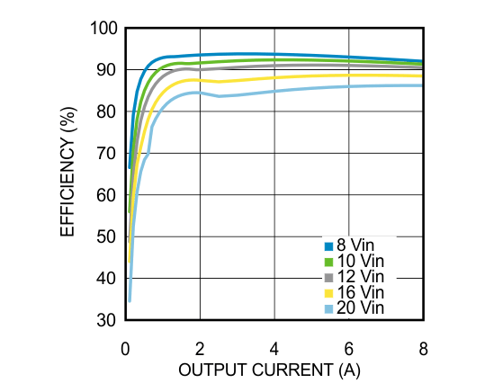
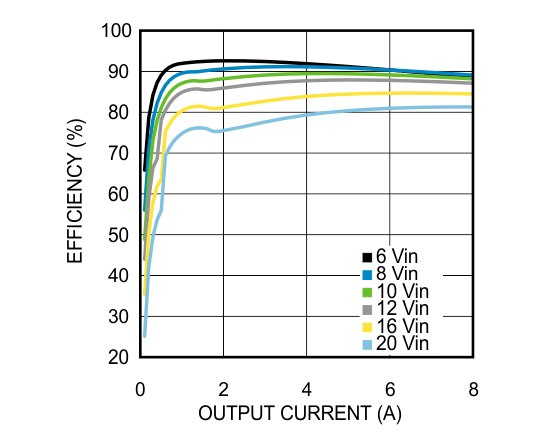
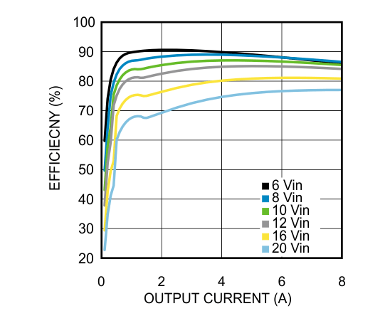
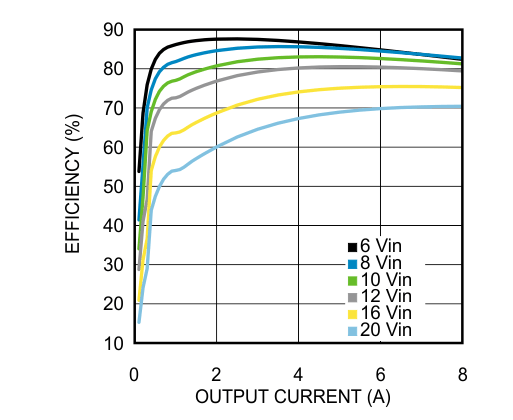
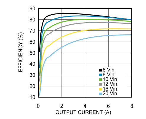
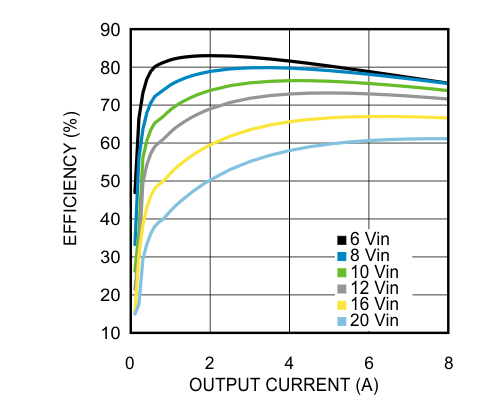
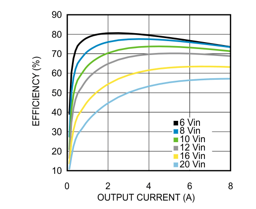
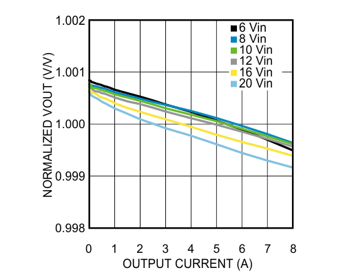
| VOUT = 3.3 V |
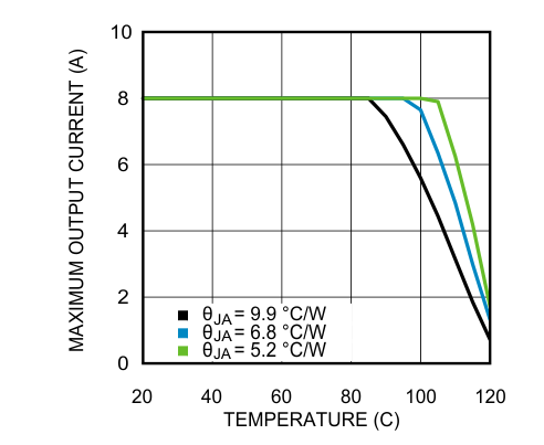
| VIN = 12 V, VOUT = 3.3 V |
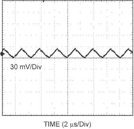
| 12 VIN, 5 VOUT at Full Load, BW = 20 MHz |
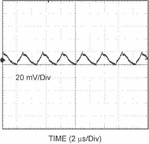
| 12 VIN, 3.3 VOUT at Full Load, BW = 20 MHz |
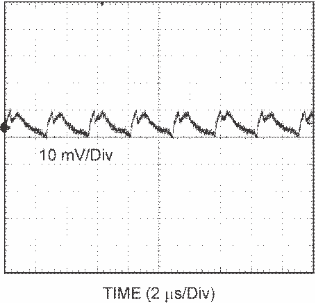
| 12 VIN, 1.2 VOUT at Full Load, BW = 20 MHz |
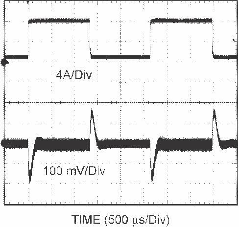
| 12 VIN, 5 VOUT 1- to 8-A Step |
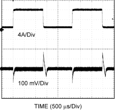
| 12 VIN, 1.2 VOUT 1- to 8-A Step |
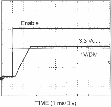
| No CSS |
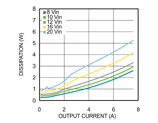
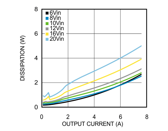
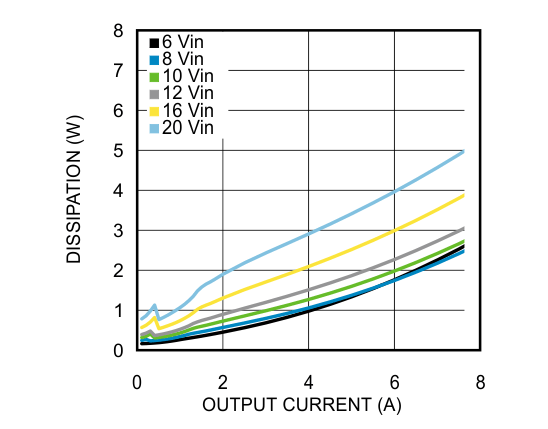
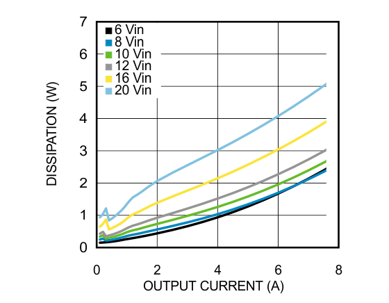
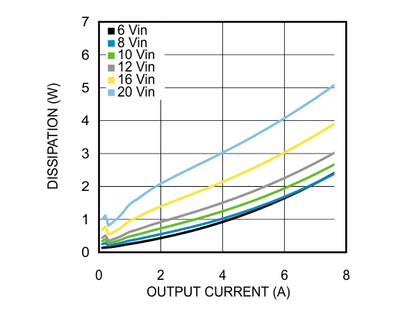
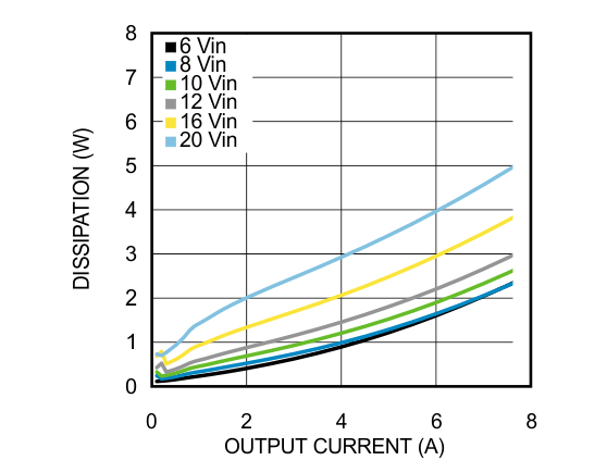
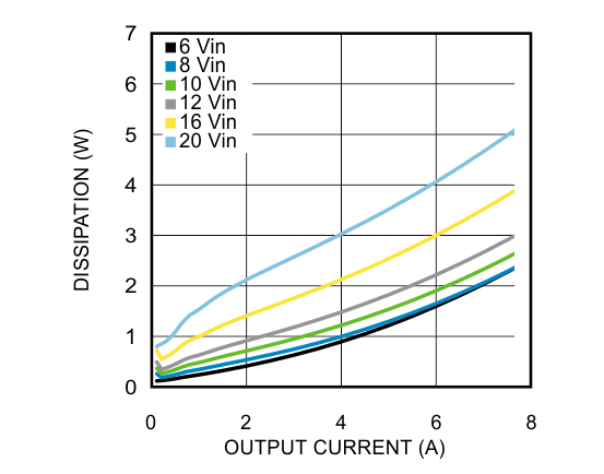
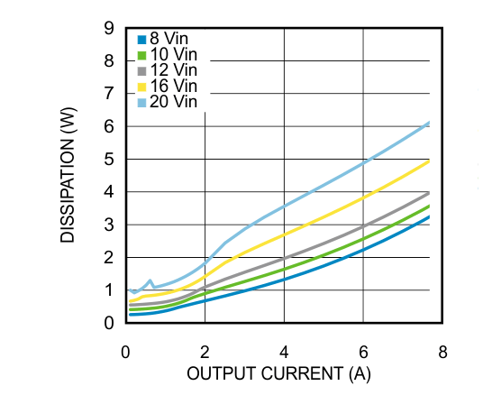
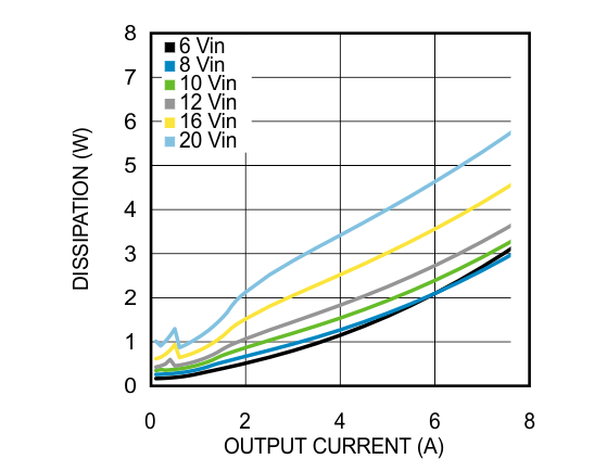
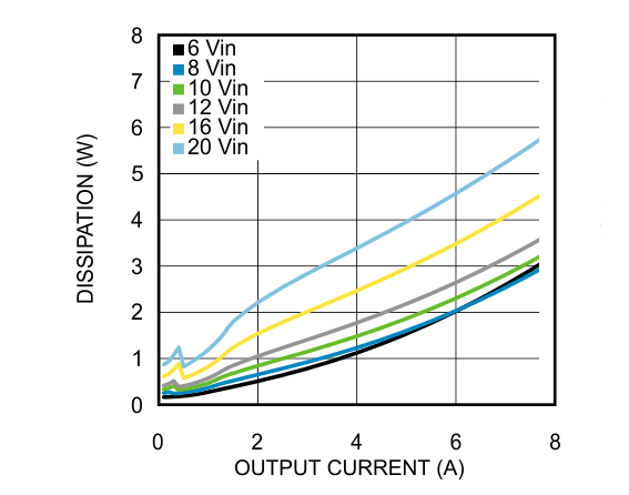


| VIN = 12 V, VOUT = 5 V |
| 12 VIN, 5 VOUT at Full Load, BW = 250 MHz |
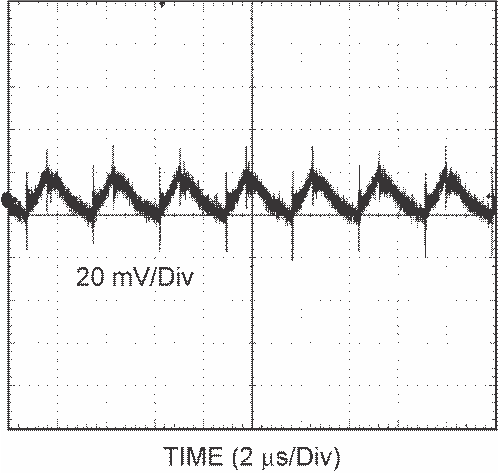
| 12 VIN, 3.3 VOUT at Full Load, BW = 250 MHz |
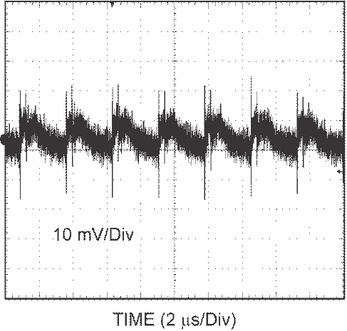
| 12 VIN, 1.2 VOUT at Full Load, BW = 250 MHz |
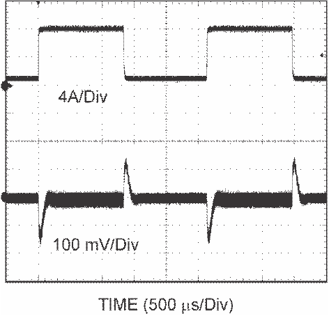
| 12 VIN, 3.3 VOUT 1- to 8-A Step |
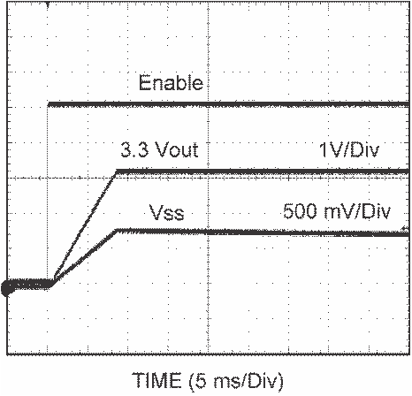
| CSS = 0.47 µF |