SNVS658I March 2011 – August 2015 LMZ22003
PRODUCTION DATA.
- 1 Features
- 2 Applications
- 3 Description
- 4 Revision History
- 5 Pin Configuration and Functions
- 6 Specifications
- 7 Detailed Description
-
8 Application and Implementation
- 8.1 Application Information
- 8.2
Typical Application
- 8.2.1 Design Requirements
- 8.2.2
Detailed Design Procedure
- 8.2.2.1 Design Steps
- 8.2.2.2 Enable Divider, RENT, RENB and RENHSelection
- 8.2.2.3 Output Voltage Selection
- 8.2.2.4 Soft-Start Capacitor Selection
- 8.2.2.5 Tracking Supply Divider Option
- 8.2.2.6 CO Selection
- 8.2.2.7 CIN Selection
- 8.2.2.8 Discontinuous Conduction and Continuous Conduction Modes Selection
- 8.2.3 Application Curves
- 9 Power Supply Recommendations
- 10Layout
- 11Device and Documentation Support
- 12Mechanical, Packaging, and Orderable Information
Package Options
Mechanical Data (Package|Pins)
- NDW|7
Thermal pad, mechanical data (Package|Pins)
Orderable Information
10 Layout
10.1 Layout Guidelines
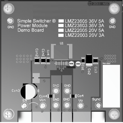
PCB layout is an important part of DC-DC converter design. Poor board layout can disrupt the performance of a DC-DC converter and surrounding circuitry by contributing to EMI, ground bounce and resistive voltage drop in the traces. These can send erroneous signals to the DC-DC converter resulting in poor regulation or instability. Good layout can be implemented by following a few simple design rules. A good example layout is shown in Figure 54.
10.2 Layout Examples
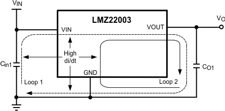 Figure 52. Critical Current Loops to Minimize
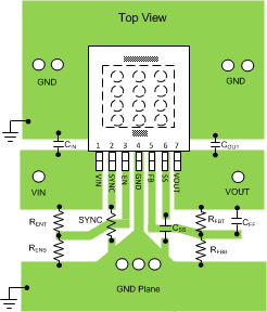 Figure 53. PCB Layout Guide
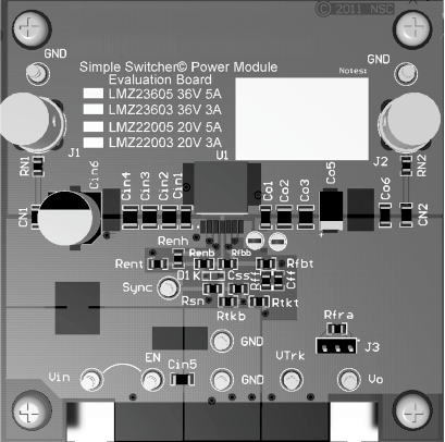 Figure 54. Top View Evaluation Board – See AN–2085
10.3 Power Dissipation and Thermal Considerations
When calculating module dissipation use the maximum input voltage and the average output current for the application. Many common operating conditions are provided in the characteristic curves such that less common applications can be derived through interpolation. In all designs, the junction temperature must be kept below the rated maximum of 125°C.
For the design case of VIN = 12 V, VO = 3.3 V, IO = 3 A, and TAMB(MAX) = 85°C, the module must see a thermal resistance from case to ambient of less than:
Given the typical thermal resistance from junction to case to be 1.9°C/W. Use the 85°C power dissipation curves in the Typical Characteristics section to estimate the PIC-LOSS for the application being designed. In this application it is 2W.
To reach RθCA = 18.1, the PCB is required to dissipate heat effectively. With no airflow and no external heat-sink, a good estimate of the required board area covered by 2-oz. copper on both the top and bottom metal layers is:
As a result, approximately 28 square cm of 2-oz. copper on top and bottom layers is required for the PCB design. The PCB copper heat sink must be connected to the exposed pad. Approximately sixty, 8 mil thermal vias spaced 39 mils (1.0 mm) apart connect the top copper to the bottom copper. For an example of a high thermal performance PCB layout for SIMPLE SWITCHER power modules, refer to AN-2085 (SNVA457), AN-2125 (SNVA437), AN-2020 (SNVA419) and AN-2026 (SNVA424).
10.4 Power Module SMT Guidelines
The recommendations below are for a standard module surface mount assembly
- Land Pattern — Follow the PCB land pattern with either soldermask defined or non-soldermask defined pads
- Stencil Aperture
- For the exposed die attach pad (DAP), adjust the stencil for approximately 80% coverage of the PCB land pattern
- For all other I/O pads use a 1:1 ratio between the aperture and the land pattern recommendation
- Solder Paste — Use a standard SAC Alloy such as SAC 305, type 3 or higher
- Stencil Thickness — 0.125 to 0.15mm
- Reflow - Refer to solder paste supplier recommendation and optimized per board size and density
- Refer to Design Summary LMZ1xxx and LMZ2xxx Power Modules Family (SNAA214) for reflow information
- Maximum number of reflows allowed is one
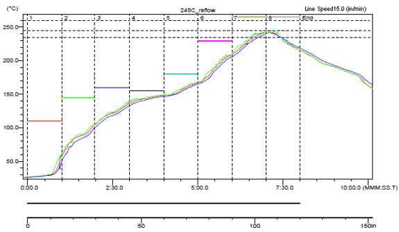 Figure 56. Sample Reflow Profile
Table 2. Sample Reflow Profile Table
| PROBE | MAX TEMP (°C) | REACHED MAX TEMP | TIME ABOVE 235°C | REACHED 235°C | TIME ABOVE 245°C | REACHED 245°C | TIME ABOVE 260°C | REACHED 260°C |
|---|---|---|---|---|---|---|---|---|
| 1 | 242.5 | 6.58 | 0.49 | 6.39 | 0.00 | – | 0.00 | – |
| 2 | 242.5 | 7.10 | 0.55 | 6.31 | 0.00 | 7.10 | 0.00 | – |
| 3 | 241.0 | 7.09 | 0.42 | 6.44 | 0.00 | – | 0.00 | – |
