SNVSAO4D December 2017 – August 2020 LMZM33602
PRODUCTION DATA
- 1Features
- 2Applications
- 3Description
- 4Revision History
- 5Pin Configuration and Functions
- 6Specifications
-
7Detailed Description
- 7.1 Overview
- 7.2 Functional Block Diagram
- 7.3
Feature Description
- 7.3.1 Adjusting the Output Voltage
- 7.3.2 Feedforward Capacitor, CFF
- 7.3.3 Voltage Dropout
- 7.3.4 Switching Frequency (RT)
- 7.3.5 Synchronization (SYNC)
- 7.3.6 Input Capacitors
- 7.3.7 Output Capacitors
- 7.3.8 Output On/Off Enable (EN)
- 7.3.9 Programmable Undervoltage Lockout (UVLO)
- 7.3.10 Power Good (PGOOD)
- 7.3.11 Overcurrent Protection (OCP)
- 7.3.12 Thermal Shutdown
- 7.4 Device Functional Modes
- 8Application and Implementation
- 9Device and Documentation Support
Package Options
Mechanical Data (Package|Pins)
- RLR|18
Thermal pad, mechanical data (Package|Pins)
Orderable Information
7.3.1 Adjusting the Output Voltage
A resistor divider connected to the FB pin (pin 16) programs the output voltage of the LMZM33602. The output voltage adjustment range is from 1 V to 18 V. Figure 7-1 shows the feedback resistor connections for setting the output voltage. The recommended value of RFBB is 10 kΩ. The value for RFBT can be calculated using Equation 1. Depending on the output voltage, a feedforward capacitor, CFF, can be required for optimum transient performance. Table 7-1 lists the standard external RFBT and CFF values for several output voltages between 2.5 V and 18 V. Table 7-2 lists the values for output voltages below 2.5 V. Additionally, Table 7-1 and Table 7-2 include the recommended switching frequency (FSW), the frequency setting resistor (RRT), and the minimum and maximum output capacitance for each of the output voltages listed.
For designs with RFBB other than 10 kΩ, adjust CFF and RFBT such that (CFF × RFBT) is unchanged and adjust RFBT such that (RFBT / RFBB) is unchanged.
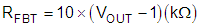
 Figure 7-1 Setting the Output Voltage
| VOUT (V) | RFBT (kΩ)(3) | CFF (pF) | fSW (kHz) | RRT (kΩ) | COUT(min) (µF)(1) | COUT(max) (µF)(2) |
|---|---|---|---|---|---|---|
| 2.5 | 15.0 | 220 | 250 | 162 | 150 | 400 |
| 3.3 | 23.2 | 150 | 300 | 133 | 88 | 300 |
| 5 | 40.2 | 100 | 450 | 88.7 | 66 | 200 |
| 6 | 49.9 | 68 | 550 | 71.5 | 54 | 160 |
| 7.5 | 64.9 | 47 | 650 | 60.4 | 40 | 130 |
| 9 | 80.6 | 47 | 700 | 56.2 | 36 | 110 |
| 12 | 110 | open | 900 | 44.2 | 22 | 80 |
| 13.5 | 124 | open | 1000 | 39.2 | 22 | 75 |
| 15 | 140 | open | 1100 | 35.7 | 20 | 65 |
| 18 | 169 | open | 1200 | 33.2 | 16 | 55 |
| VOUT (V) | RFBT (kΩ)(1) | CFF (pF) | FSW (kHz) | RRT (kΩ) | COUT |
|---|---|---|---|---|---|
| 1 to 2.5 | See Equation 1 | open | 250 | 162 | 150-µF ceramic + 470-µF polymer |