SNVSAO6C September 2017 – March 2018 LMZM33603
PRODUCTION DATA.
- 1 Features
- 2 Applications
- 3 Description
- 4 Revision History
- 5 Pin Configuration and Functions
- 6 Specifications
-
7 Detailed Description
- 7.1 Overview
- 7.2 Functional Block Diagram
- 7.3
Feature Description
- 7.3.1 Adjusting the Output Voltage
- 7.3.2 Feed-Forward Capacitor, CFF
- 7.3.3 Output Current vs Output Voltage
- 7.3.4 Voltage Dropout
- 7.3.5 Switching Frequency (RT)
- 7.3.6 Synchronization (SYNC)
- 7.3.7 Input Capacitors
- 7.3.8 Output Capacitors
- 7.3.9 Output On/Off Enable (EN)
- 7.3.10 Programmable Undervoltage Lockout (UVLO)
- 7.3.11 Power Good (PGOOD)
- 7.3.12 Overcurrent Protection (OCP)
- 7.3.13 Thermal Shutdown
- 7.4 Device Functional Modes
- 8 Application and Implementation
- 9 Power Supply Recommendations
- 10Layout
- 11Device and Documentation Support
- 12Mechanical, Packaging, and Orderable Information
Package Options
Mechanical Data (Package|Pins)
- RLR|18
Thermal pad, mechanical data (Package|Pins)
Orderable Information
5 Pin Configuration and Functions
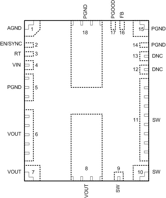
RLR Package
18-Pin QFN
Top View

Pin Functions
| PIN | TYPE | DESCRIPTION | |
|---|---|---|---|
| NO. | NAME | ||
| 1 | AGND | G | Analog ground. Zero voltage reference for internal references and logic. Do not connect this pin to PGND; the connection is made internal to the device. See the Layout section of the datasheet for a recommended layout. |
| 2 | EN/SYNC | I | EN - Enable input to regulator. High = On, Low = Off. Can be connected to VIN. Do not float. This pin can be used to set the input under voltage lockout with two resistors. See the Programmable Undervoltage Lockout (UVLO) section.
SYNC - The internal oscillator can be synchronized to an external clock via AC-coupling. See the Synchronization (SYNC) section for details. |
| 3 | RT | I | An external timing resistor connected between this pin and AGND adjusts the switching frequency of the device. If left open, the default switching frequency is 400 kHz. |
| 4 | VIN | I | Input supply voltage. Connect external input capacitors between this pin and PGND. |
| 5, 14, 15, 18 | PGND | G | Power ground. This is the return current path for the power stage of the device. Connect pin 5 to the input source, the load, and to the bypass capacitors associated with VIN and VOUT using power ground planes on the PCB. Pins 14 and 15 are not connected to PGND internal to the device and must be connected to PGND at pad 18. Connect pad 18 to the power ground planes using multiple vias for good thermal performance. See the Layout section of the datasheet for a recommended layout. |
| 6, 7, 8 | VOUT | O | Output voltage. These pins are connected to the internal output inductor. Connect these pins to the output load and connect external bypass capacitors between these pins and PGND. |
| 9, 10, 11 | SW | O | Switch node. Connect these pins to a small copper island under the device for thermal relief. Do not place any external component on these pins or tie them to a pin of another function. |
| 12, 13 | DNC | — | Do not connect. Each pin must be soldered to an isolated pad. These pins connect to internal circuitry. Do not connect these pins to one another, AGND, PGND, or any other voltage. |
| 16 | FB | I | Feedback input. Connect the center point of the feedback resistor divider to this pin. Connect the upper resistor (RFBT) of the feedback divider to VOUT at the desired point of regulation. Connect the lower resistor (RFBB) of the feedback divider to AGND. |
| 17 | PGOOD | O | Open drain output for power-good flag. Use a 10-kΩ to 100-kΩ pullup resistor to logic rail or other DC voltage no higher than 12 V. |