SNOS510Q November   1999  – October 2016 LP2985LV-N

PRODUCTION DATA.  

  1. Features
  2. Applications
  3. Description
  4. Revision History
  5. Pin Configuration and Functions
  6. Specifications
    1. 6.1 Absolute Maximum Ratings
    2. 6.2 ESD Ratings
    3. 6.3 Recommended Operating Conditions
    4. 6.4 Thermal Information
    5. 6.5 Electrical Characteristics
    6. 6.6 Typical Characteristics
  7. Detailed Description
    1. 7.1 Overview
    2. 7.2 Functional Block Diagram
    3. 7.3 Feature Description
      1. 7.3.1 Multiple Voltage Options
      2. 7.3.2 Output Voltage Accuracy
      3. 7.3.3 Ultra-Low-Dropout Voltage
      4. 7.3.4 Low Ground Current
      5. 7.3.5 Sleep Mode
      6. 7.3.6 Internal Protection Circuitry
        1. 7.3.6.1 Short Circuit Protection (Current Limit)
        2. 7.3.6.2 Thermal Protection
      7. 7.3.7 Enhanced Stability
      8. 7.3.8 Low Noise
    4. 7.4 Device Functional Modes
      1. 7.4.1 Operation with VOUT(TARGET) + 0.6 V ≥ VIN > 16 V
      2. 7.4.2 Operation With ON/OFF Control
  8. Application and Implementation
    1. 8.1 Application Information
    2. 8.2 Typical Application
      1. 8.2.1 Design Requirements
      2. 8.2.2 Detailed Design Procedure
        1. 8.2.2.1 External Capacitors
          1. 8.2.2.1.1 Input Capacitor
          2. 8.2.2.1.2 Output Capacitor
          3. 8.2.2.1.3 Noise Bypass Capacitor
        2. 8.2.2.2 Capacitor Characteristics
          1. 8.2.2.2.1 Tantalum
        3. 8.2.2.3 On/OFF Input Operation
        4. 8.2.2.4 Reverse Input-Output Voltage
        5. 8.2.2.5 Power Dissipation
        6. 8.2.2.6 Estimating Junction Temperature
      3. 8.2.3 Application Curves
  9. Power Supply Recommendations
  10. 10Layout
    1. 10.1 Layout Guidelines
    2. 10.2 Layout Example
    3. 10.3 DSBGA Mounting
    4. 10.4 DSBGA Light Sensitivity
  11. 11Device and Documentation Support
    1. 11.1 Documentation Support
      1. 11.1.1 Related Documentation
      2. 11.1.2 Receiving Notification of Documentation Updates
    2. 11.2 Community Resources
    3. 11.3 Trademarks
    4. 11.4 Electrostatic Discharge Caution
    5. 11.5 Glossary
  12. 12Mechanical, Packaging, and Orderable Information

Package Options

Mechanical Data (Package|Pins)
Thermal pad, mechanical data (Package|Pins)
Orderable Information

Pin Configuration and Functions

DBV Package
5 Pin SOT-23
Top View
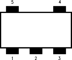
LP2985LV-N 10129503.png
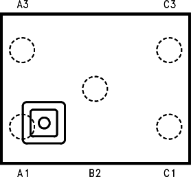
YPB Package
5-Pin DSBGA
Top View
LP2985LV-N 10129523.png
The actual physical placement of the package marking varies from part to part. Package marking contains date code and lot traceability information and will vary considerably. Package marking does not correlate to device type.

Pin Functions

PIN TYPE DESCRIPTION
NAME SOT-23 DSBGA
BYPASS 4 B2 I/O Bypass capacitor for low noise operation
GND 2 A1 Common ground (device substrate)
IN 1 C3 I Input voltage
ON/OFF 3 A3 I Logic high enable input
OUT 5 C1 O Regulated output voltage