SNVS137I March 1999 – September 2015 LP2986
PRODUCTION DATA.
- 1 Features
- 2 Applications
- 3 Description
- 4 Revision History
- 5 Pin Configuration and Function
- 6 Specifications
- 7 Detailed Description
- 8 Application and Implementation
- 9 Power Supply Recommendations
- 10Layout
- 11Device and Documentation Support
- 12Mechanical, Packaging, and Orderable Information
Package Options
Mechanical Data (Package|Pins)
Thermal pad, mechanical data (Package|Pins)
Orderable Information
8 Application and Implementation
NOTE
Information in the following applications sections is not part of the TI component specification, and TI does not warrant its accuracy or completeness. TI’s customers are responsible for determining suitability of components for their purposes. Customers should validate and test their design implementation to confirm system functionality.
8.1 Application Information
The LP2986 can provide 200-mA output current with 2.1-V to 16-V input. It is stable with a minimum of 4.7-µF ceramic output capacitor. An input capacitor of (≥ 2.2 μF) is required. An optional external bypass capacitor reduces the output noise without slowing down the load transient response. Typical output noise is 160 µVRMS at frequencies from 300 Hz to 50 kHz. Typical power supply rejection is 65 dB at 1 kHz.
8.2 Typical Applications
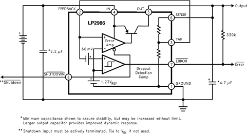 Figure 29. Application Using Internal Resistive Divider
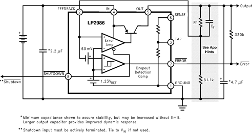 Figure 30. Application Using External Divider
8.2.1 Design Requirements
For typical ultra-low-dropout linear regulator applications, use the parameters listed in Table 1.
Table 1. Design Parameters
| DESIGN PARAMETER | EXAMPLE VALUE |
|---|---|
| Input voltage | 4.3 V |
| Output voltage | 3.3 V |
| Output current | 200 mA (maximum) |
| RMS noise, 300 Hz to 50 kHz | 150 µVRMS typical |
| PSRR at 1 kHz | 65 dB typical |
8.2.2 Detailed Design Procedure
8.2.2.1 Using an External Resistive Divider
The LP2986 output voltage can be programmed using an external resistive divider. Figure 30 shows a typical circuit application using external resistive divider.
The resistor connected between the FEEDBACK pin and ground should be 51.1 kΩ. The value for the other resistor (R1) connected between the FEEDBACK pin and the regulated output is found using the formula:
It should be noted that the 25 µA of current flowing through the external divider is approximately equal to the current saved by not connecting the internal divider, which means the quiescent current is not increased by using external resistors.
A lead compensation capacitor (CF) must also be used to place a zero in the loop response at about 50 kHz. The value for C F can be found using:
A good quality capacitor must be used for CF to ensure that the value is accurate and does not change significantly over temperature. Mica or ceramic capacitors can be used, assuming a tolerance of ±20% or better is selected.
If a ceramic is used, select one with a temperature coefficient of NPO, COG, Y5P, or X7R. Capacitor types Z5U, Y5V, and Z4V can not be used because their value varies more that 50% over the −25°C to +85°C temperature range.
8.2.2.2 External Capacitors
Like any low-dropout regulator, external capacitors are required to assure stability. These capacitors must be correctly selected for proper performance.
8.2.2.2.1 Input Capacitor
An input capacitor (≥ 2.2 µF) is required between the LP2986 input and ground (amount of capacitance may be increased without limit).
This capacitor must be located a distance of not more than 0.5 inches from the input pin and returned to a clean analog ground. Any good quality ceramic or tantalum may be used for this capacitor.
8.2.2.2.2 Output Capacitor
The output capacitor must meet the requirement for minimum amount of capacitance and also have an appropriate equivalent series resistance (ESR) value.
Curves are provided which show the allowable ESR range as a function of load current for various output voltages and capacitor values (see Figure 31 and Figure 32).
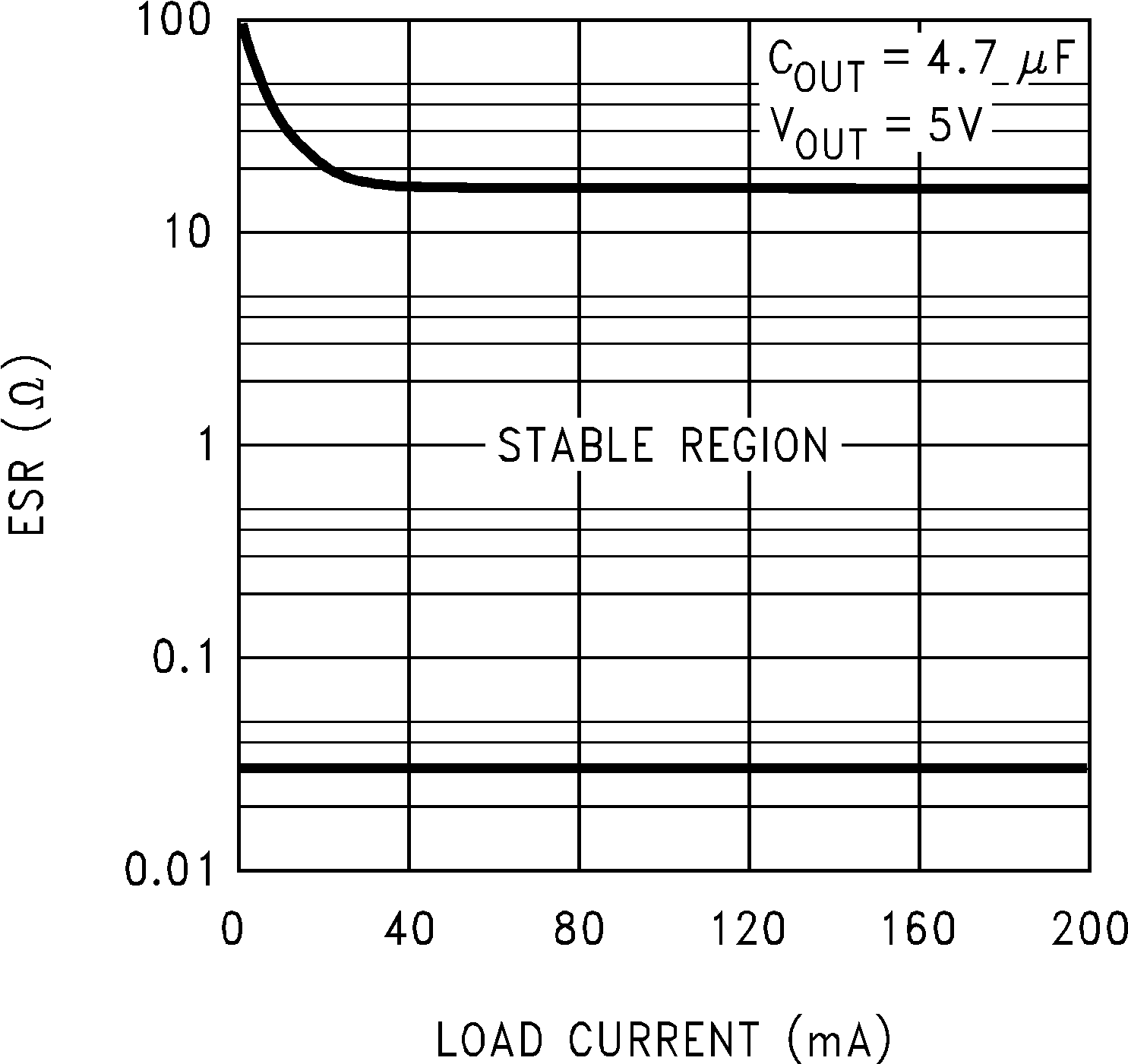 Figure 31. ESR Curves For 5-V Output
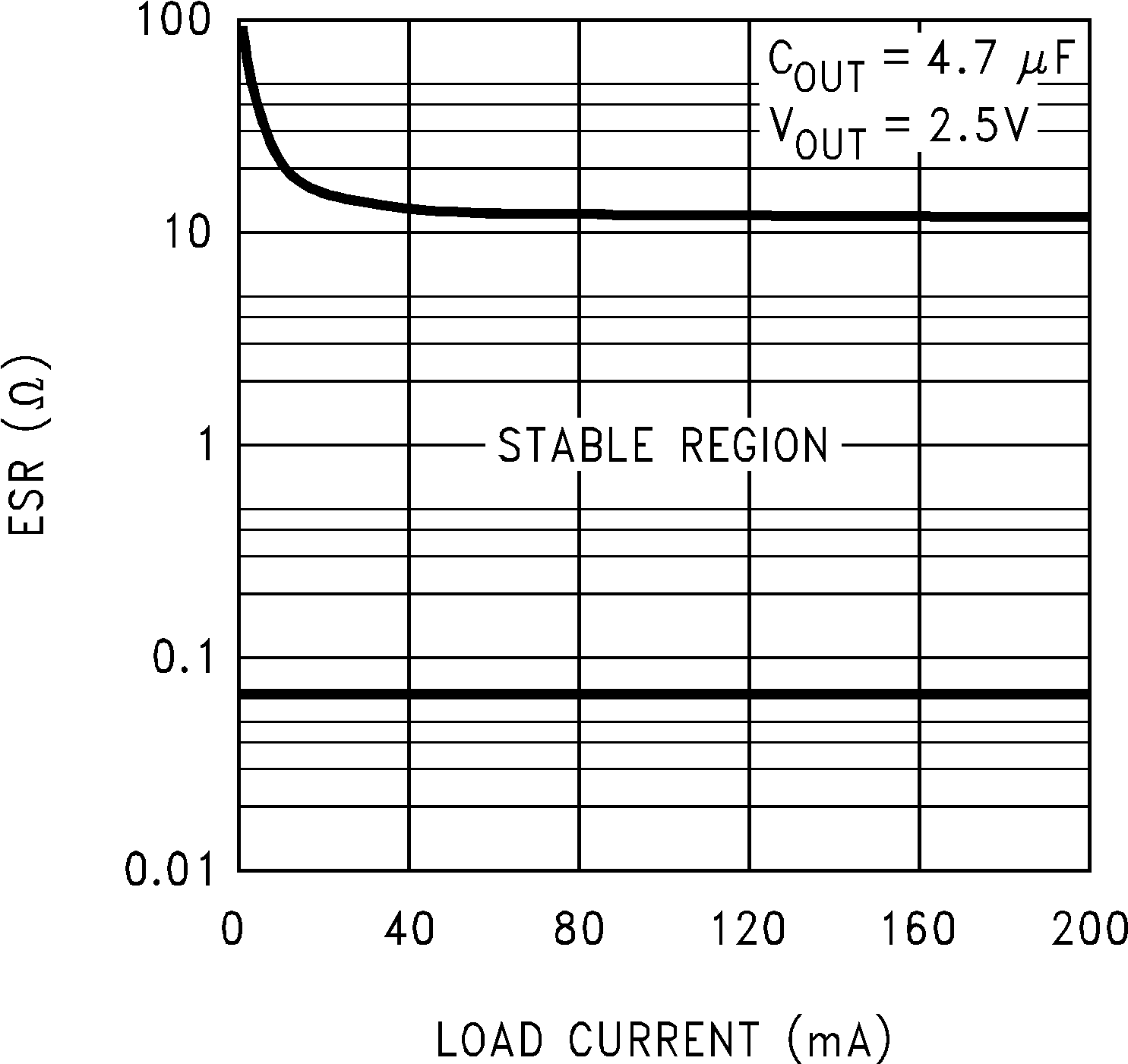 Figure 32. ESR Curves for 2.5-V Output
NOTE
The output capacitor must maintain its ESR in the stable region over the full operating temperature range of the application to assure stability.
The minimum required amount of output capacitance is 4.7 µF. Output capacitor size can be increased without limit.
It is important to remember that capacitor tolerance and variation with temperature must be taken into consideration when selecting an output capacitor so that the minimum required amount of output capacitance is provided over the full operating temperature range. A good tantalum capacitor will show very little variation with temperature, but a ceramic may not be as good (see Capacitor Characteristics).
8.2.2.3 Capacitor Characteristics
8.2.2.3.1 Tantalum
The best choice for size, cost, and performance are solid tantalum capacitors. Available from many sources, their typical ESR is very close to the ideal value required on the output of many LDO regulators.
Tantalums also have good temperature stability: a 4.7 µF was tested and showed only a 10% decline in capacitance as the temperature was decreased from +125°C to −40°C. The ESR increased only about 2:1 over the same range of temperature.
However, it should be noted that the increasing ESR at lower temperatures present in all tantalums can cause oscillations when marginal quality capacitors are used (where the ESR of the capacitor is near the upper limit of the stability range at room temperature).
8.2.2.3.2 Ceramic
For a given amount of a capacitance, ceramics are usually larger and more costly than tantalums.
Be warned that the ESR of a ceramic capacitor can be low enough to cause instability: a 2.2-µF ceramic capacitor was measured and found to have an ESR of about 15 mΩ.
If a ceramic capacitor is to be used on the LP2986 output, a 1-Ω resistor should be placed in series with the capacitor to provide a minimum ESR for the regulator.
Another disadvantage of ceramic capacitors is that their capacitance varies a lot with temperature:
Large ceramic capacitors are typically manufactured with the Z5U temperature characteristic, which results in the capacitance dropping by a 50% as the temperature goes from +25°C to 80°C.
This means you have to buy a capacitor with twice the minimum COUT to assure stable operation up to 80°C.
8.2.2.3.3 Aluminum
The large physical size of aluminum electrolytics makes them unattractive for use with the LP2986. Their ESR characteristics are also not well suited to the requirements of LDO regulators.
The ESR of an aluminum electrolytic is higher than a tantalum, and it also varies greatly with temperature.
A typical aluminum electrolytic can exhibit an ESR increase of 50× when going from +20°C to −40°C. Also, some aluminum electrolytics can not be used below −25°C because the electrolyte will freeze.
8.2.2.4 Reverse Input-Output Voltage
The PNP power transistor used as the pass element in the LP2986 has an inherent diode connected between the regulator output and input.
During normal operation (where the input voltage is higher than the output) this diode is reverse-biased.
However, if the output voltage is pulled above the input, or the input voltage is pulled below the output, this diode will turn ON and current will flow into the regulator OUT pin.
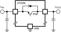 Figure 33. Inherent Diode
In such cases, a parasitic SCR can latch which will allow a high current to flow into VIN (and out the GROUND pin), which can damage the part.
In any application where the output voltage may be higher than the input, an external Schottky diode must be connected from VIN to VOUT (cathode on VIN, anode on VOUT), to limit the reverse voltage across the LP2986 to 0.3 V (see Absolute Maximum Ratings).
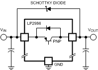 Figure 34. Inherent and External Schottky Diodes
8.2.2.5 WSON Package Devices
The LP2986 is offered in the 8-pin WSON surface mount package to allow for increased power dissipation compared to the 8-pin SOIC-8 and 8-pin VSSOP. For details on WSON thermal performance as well as mounting and soldering specifications, refer to WSON Mounting.
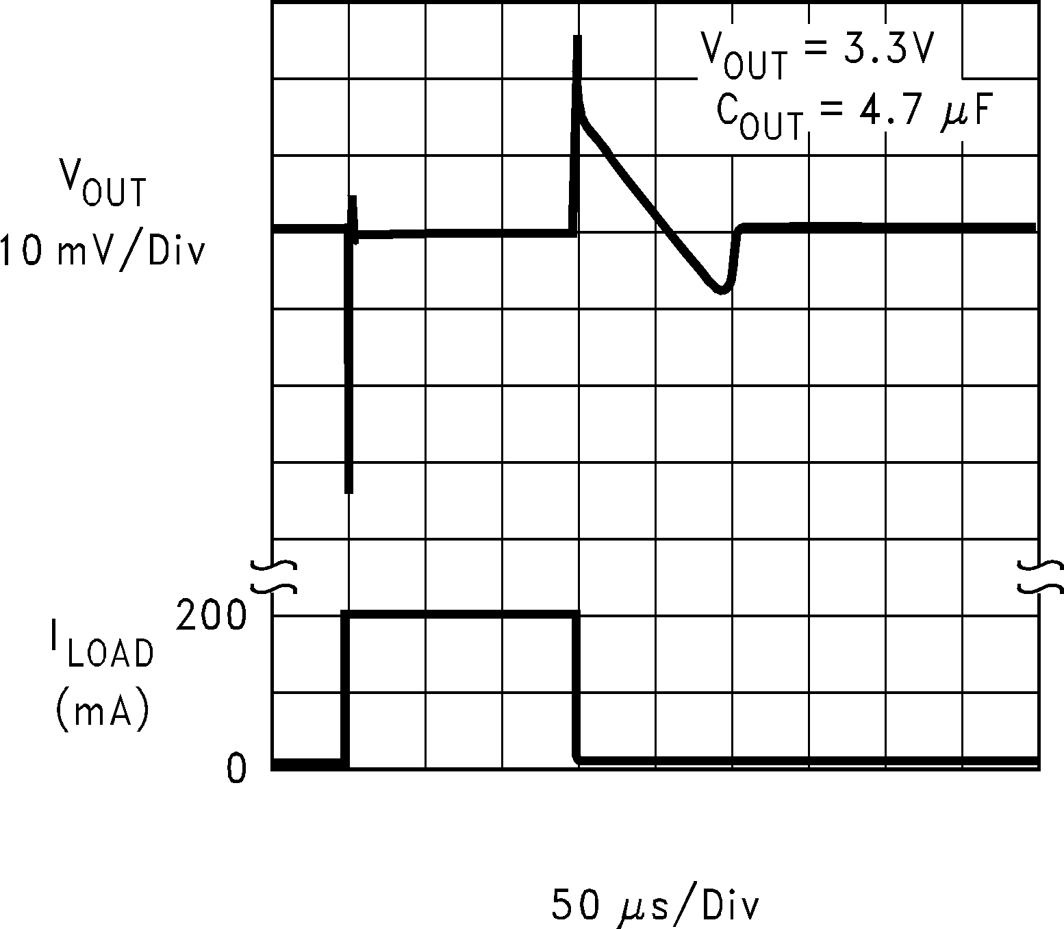
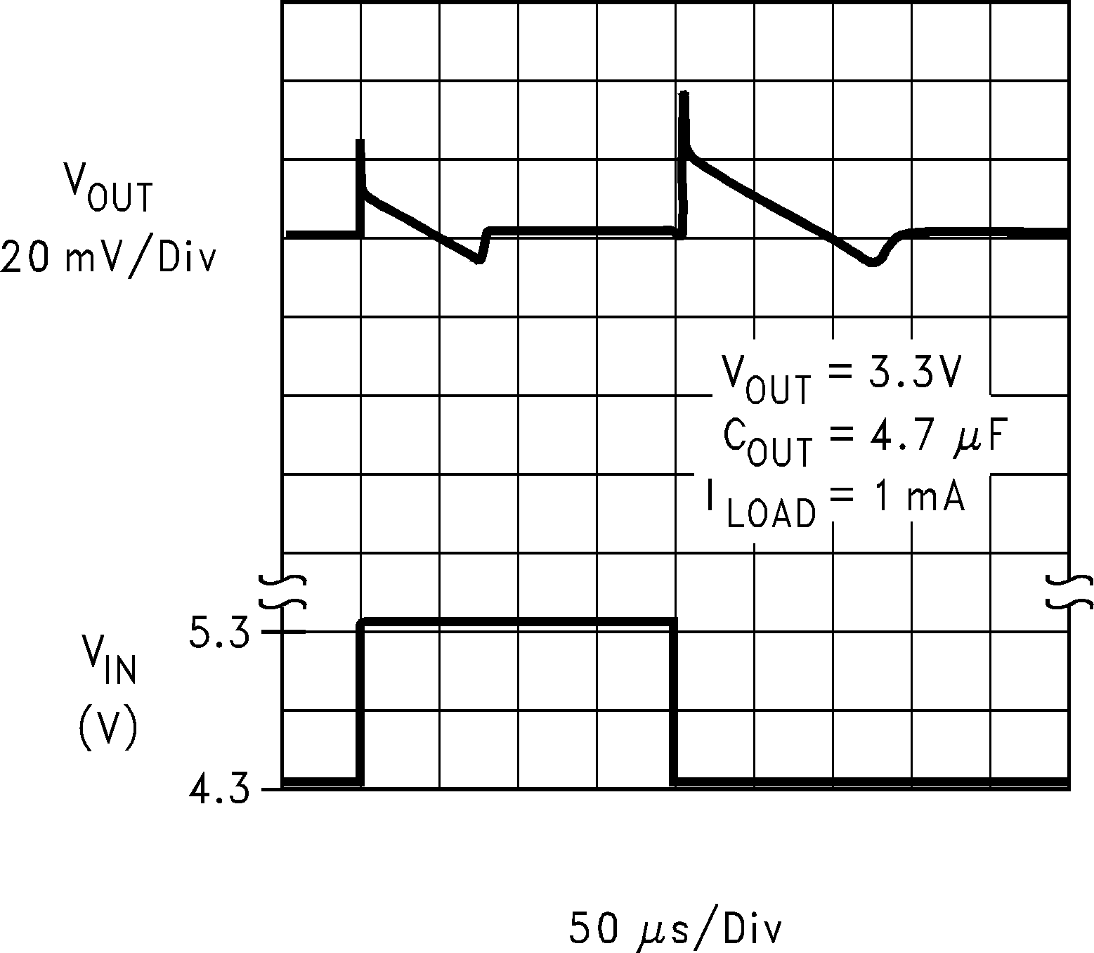
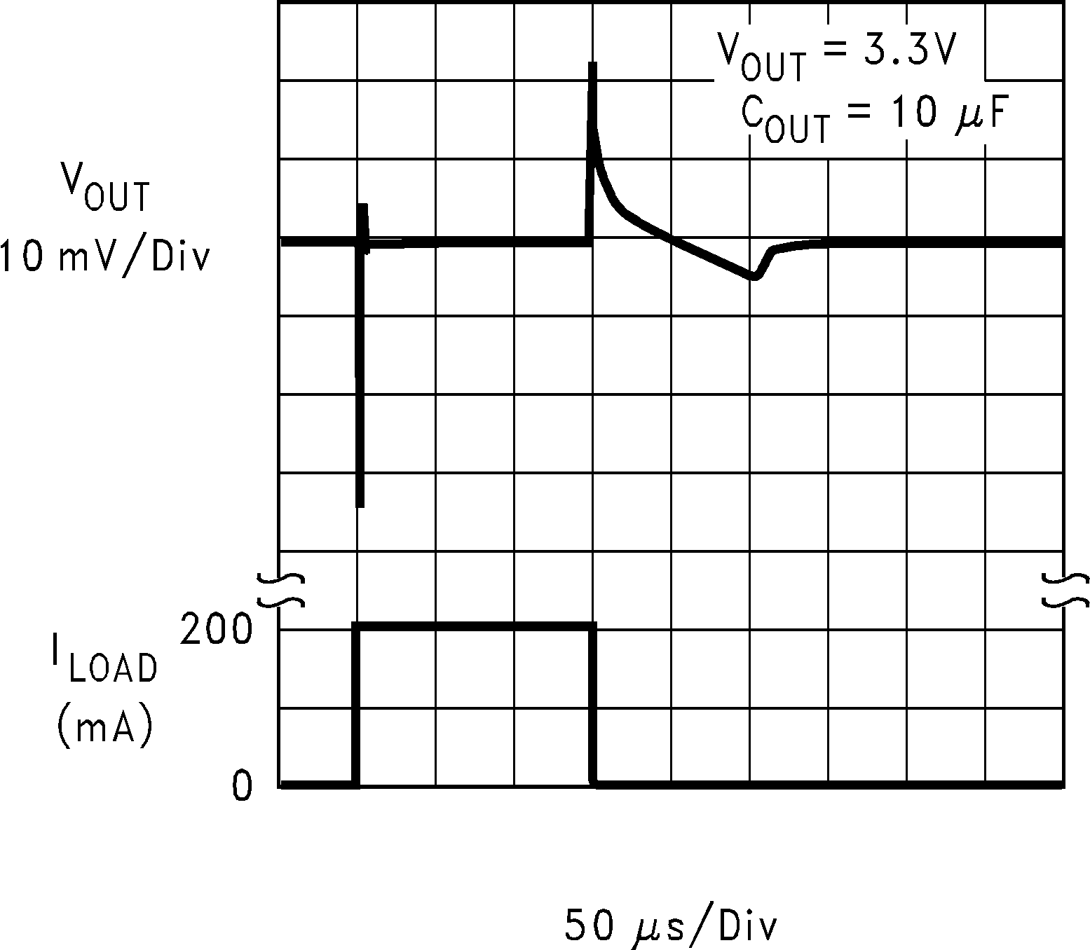
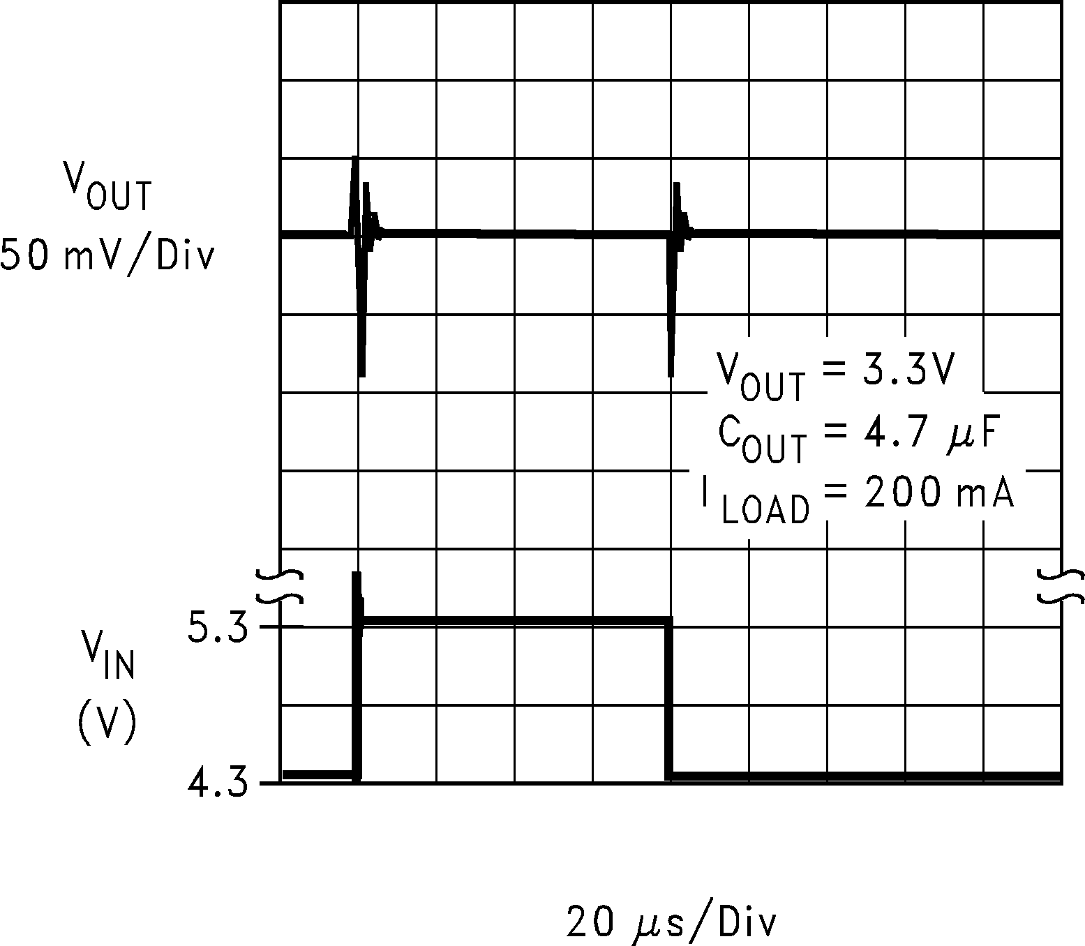
8.2.3 Application Curves
