SNVS521K December 2007 – August 2014 LP2998 , LP2998-Q1
PRODUCTION DATA.
- 1 Features
- 2 Applications
- 3 Description
- 4 Simplified Schematic
- 5 Revision History
- 6 Pin Configuration and Functions
- 7 Specifications
- 8 Detailed Description
- 9 Application and Implementation
- 10Power Supply Recommendations
- 11Layout
- 12Device and Documentation Support
- 13Mechanical, Packaging, and Orderable Information
Package Options
Mechanical Data (Package|Pins)
Thermal pad, mechanical data (Package|Pins)
- DDA|8
Orderable Information
8 Detailed Description
8.1 Overview
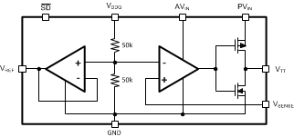
The LP2998 linear regulator is designed to meet JEDEC SSTL-2 and JEDEC SSTL-18 specifications for termination of DDR-SDRAM and DDR2 memory. The device also supports DDR3 and DDR3L VTT bus termination with VDDQ min of 1.35 V. The device contains a high-speed operational amplifier to provide excellent response to load transients. The output stage prevents shoot through while delivering 1.5 A continuous current and transient peaks up to 3 A in the application as required for DDR-SDRAM termination.
8.2 Functional Block Diagram
8.3 Feature Description
The LP2998 is a linear bus termination regulator designed to meet the JEDEC requirements of SSTL-2 and SSTL-18. The output, VTT is capable of sinking and sourcing current while regulating the output voltage equal to VDDQ / 2. The output stage has been designed to maintain excellent load regulation while preventing shoot through. The LP2998 also incorporates two distinct power rails that separates the analog circuitry from the power output stage. This allows a split rail approach to be utilized to decrease internal power dissipation. It also permits the LP2998 to provide a termination solution for DDR3-SDRAM and DDR3L-SDRAM memory.
8.4 Device Functional Modes
The LP2998 can also be used to provide a termination voltage for other logic schemes such as SSTL-3 or HSTL. Series Stub Termination Logic (SSTL) was created to improve signal integrity of the data transmission across the memory bus. This termination scheme is essential to prevent data error from signal reflections while transmitting at high frequencies encountered with DDR-SDRAM. The most common form of termination is Class II single parallel termination. This involves one RS series resistor from the chipset to the memory and one RT termination resistor. Typical values for RS and RT are 25 Ω, although these can be changed to scale the current requirements from the LP2998. This implementation can be seen below in Figure 16.
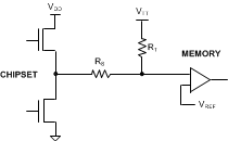 Figure 16. SSTL-Termination Scheme