SNVS521K December 2007 – August 2014 LP2998 , LP2998-Q1
PRODUCTION DATA.
- 1 Features
- 2 Applications
- 3 Description
- 4 Simplified Schematic
- 5 Revision History
- 6 Pin Configuration and Functions
- 7 Specifications
- 8 Detailed Description
- 9 Application and Implementation
- 10Power Supply Recommendations
- 11Layout
- 12Device and Documentation Support
- 13Mechanical, Packaging, and Orderable Information
Package Options
Mechanical Data (Package|Pins)
Thermal pad, mechanical data (Package|Pins)
- DDA|8
Orderable Information
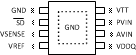
6 Pin Configuration and Functions
SO PowerPAD
8-LEAD DDA
TOP VIEW
SOIC
8-LEAD D
TOP VIEW
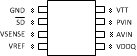
Pin Functions
| PIN | ||
|---|---|---|
| NUMBER | TYPE | DESCRIPTION |
| 1 | GND | Ground |
| 2 | SD | Shutdown |
| 3 | VSENSE | Feedback pin for regulating VTT. |
| 4 | VREF | Buffered internal reference voltage of VDDQ/2 |
| 5 | VDDQ | Input for internal reference equal to VDDQ/2 |
| 6 | AVIN | Analog input pin |
| 7 | PVIN | Power input pin |
| 8 | VTT | Output voltage for connection to termination resistors |
| EP | Exposed pad thermal connection. Connect to Ground. | |
6.1 Pin Descriptions
| AVIN AND PVIN | AVIN and PVIN are the input supply pins for the LP2998. AVIN is used to supply all the internal control circuitry. PVIN, however, is used exclusively to provide the rail voltage for the output stage used to create VTT. These pins have the capability to work off separate supplies depending on the application. Higher voltages on PVIN will increase the maximum continuous output current because of output RDSON limitations at voltages close to VTT. The disadvantage of high values of PVIN is that the internal power loss will also increase, thermally limiting the design. For SSTL-2 applications, a good compromise would be to connect the AVIN and PVIN directly together at 2.5 V. This eliminates the need for bypassing the two supply pins separately. The only limitation on input voltage selection is that PVIN must be equal to or lower than AVIN. It is recommended to connect PVIN to voltage rails equal to or less than 3.3 V to prevent the thermal limit from tripping because of excessive internal power dissipation. If the junction temperature exceeds the thermal shutdown than the part will enter a shutdown state identical to the manual shutdown where VTT is tri-stated and VREF remains active. |
| VDDQ | VDDQ is the input used to create the internal reference voltage for regulating VTT. The reference voltage is generated from a resistor divider of two internal 50 kΩ resistors. This ensures that VTT will track VDDQ / 2 precisely. The optimal implementation of VDDQ is as a remote sense. This can be achieved by connecting VDDQ directly to the 2.5 V rail at the DIMM instead of AVIN and PVIN. This ensures that the reference voltage tracks the DDR memory rails precisely without a large voltage drop from the power lines. For SSTL-2 applications VDDQ will be a 2.5 V signal, which will create a 1.25 V termination voltage at VTT (See Electrical Characteristics Table for exact values of VTT over temperature). |
|
VSENSE |
The purpose of the sense pin is to provide improved remote load regulation. In most motherboard applications the termination resistors will connect to VTT in a long plane. If the output voltage was regulated only at the output of the LP2998 then the long trace will cause a significant IR drop resulting in a termination voltage lower at one end of the bus than the other. The VSENSE pin can be used to improve this performance, by connecting it to the middle of the bus. This will provide a better distribution across the entire termination bus. If remote load regulation is not used then the VSENSE pin must still be connected to VTT. Care should be taken when a long VSENSE trace is implemented in close proximity to the memory. Noise pickup in the VSENSE trace can cause problems with precise regulation of VTT. A small 0.1 uF ceramic capacitor placed next to the VSENSE pin can help filter any high frequency signals and preventing errors. |
| SHUTDOWN | The LP2998 contains an active low shutdown pin that can be used to tri-state VTT. During shutdown VTT should not be exposed to voltages that exceed AVIN. With the shutdown pin asserted low the quiescent current of the LP2998 will drop, however, VDDQ will always maintain its constant impedance of 100 kΩ for generating the internal reference. Therefore, to calculate the total power loss in shutdown both currents need to be considered. For more information refer to the Thermal Dissipation section. The shutdown pin also has an internal pull-up current, therefore to turn the part on the shutdown pin can either be connected to AVIN or left open. |
| VREF | VREF provides the buffered output of the internal reference voltage VDDQ / 2. This output should be used to provide the reference voltage for the Northbridge chipset and memory. Since these inputs are typically an extremely high impedance, there should be little current drawn from VREF. For improved performance, an output bypass capacitor can be used, located close to the pin, to help with noise. A ceramic capacitor in the range of 0.1 µF to 0.01 µF is recommended. This output remains active during the shutdown state and thermal shutdown events for the suspend to RAM functionality. |
| VTT | VTT is the regulated output that is used to terminate the bus resistors. It is capable of sinking and sourcing current while regulating the output precisely to VDDQ / 2. The LP2998 is designed to handle peak transient currents of up to ± 3 A with a fast transient response. The maximum continuous current is a function of VIN and can be viewed in the Typical Characteristics section. If a transient is expected to last above the maximum continuous current rating for a significant amount of time then the output capacitor should be sized large enough to prevent an excessive voltage drop. Despite the fact that the LP2998 is designed to handle large transient output currents it is not capable of handling these for long durations, under all conditions. The reason for this is the standard packages are not able to thermally dissipate the heat as a result of the internal power loss. If large currents are required for longer durations, then care should be taken to ensure that the maximum junction temperature is not exceeded. Proper thermal derating should always be used (please refer to the Thermal Dissipation section). If the junction temperature exceeds the thermal shutdown point than VTT will tri-state until the part returns below the hysteretic trip-point. |