SNVS521K December 2007 – August 2014 LP2998 , LP2998-Q1
PRODUCTION DATA.
- 1 Features
- 2 Applications
- 3 Description
- 4 Simplified Schematic
- 5 Revision History
- 6 Pin Configuration and Functions
- 7 Specifications
- 8 Detailed Description
- 9 Application and Implementation
- 10Power Supply Recommendations
- 11Layout
- 12Device and Documentation Support
- 13Mechanical, Packaging, and Orderable Information
Package Options
Mechanical Data (Package|Pins)
Thermal pad, mechanical data (Package|Pins)
- DDA|8
Orderable Information
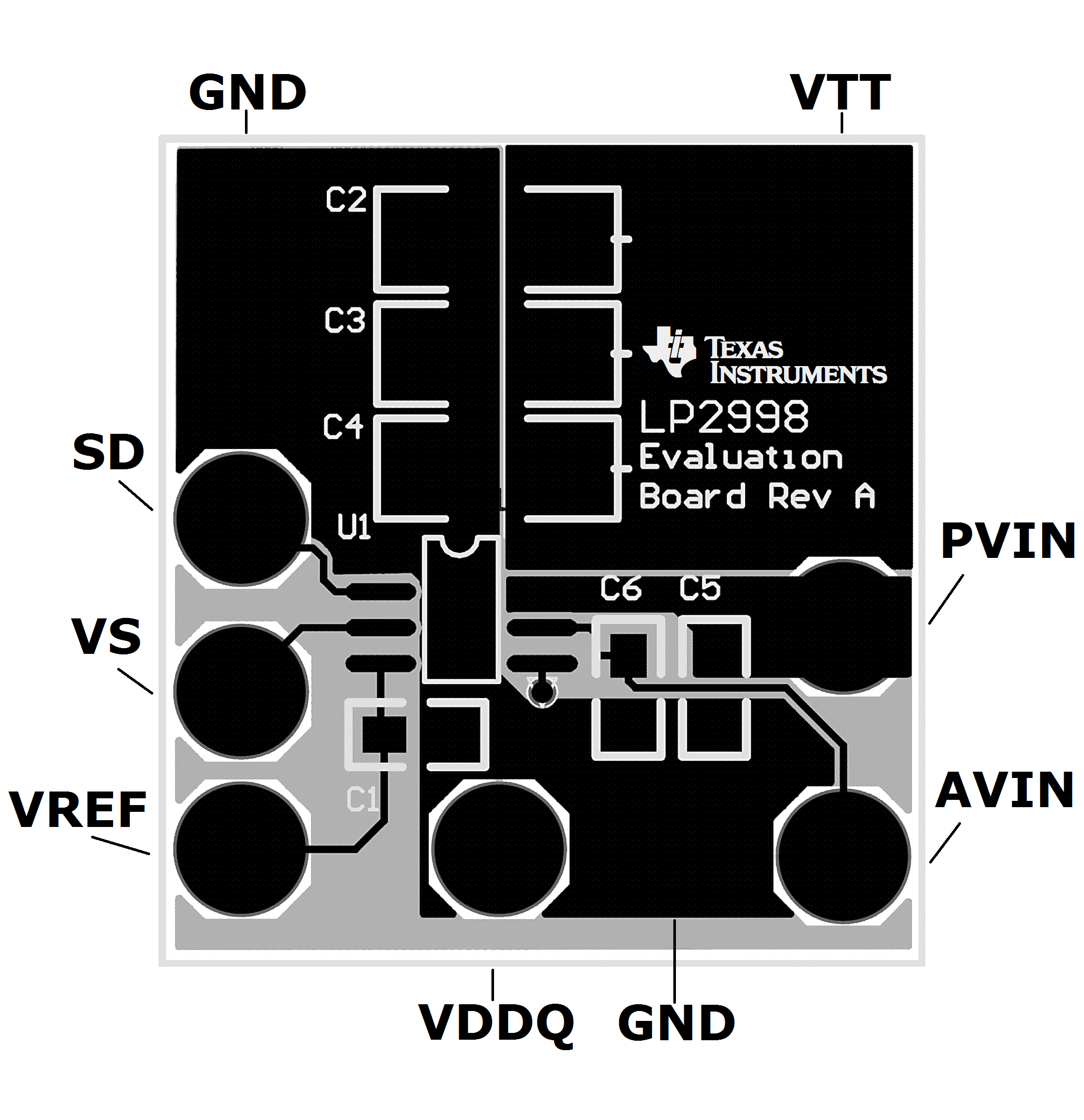
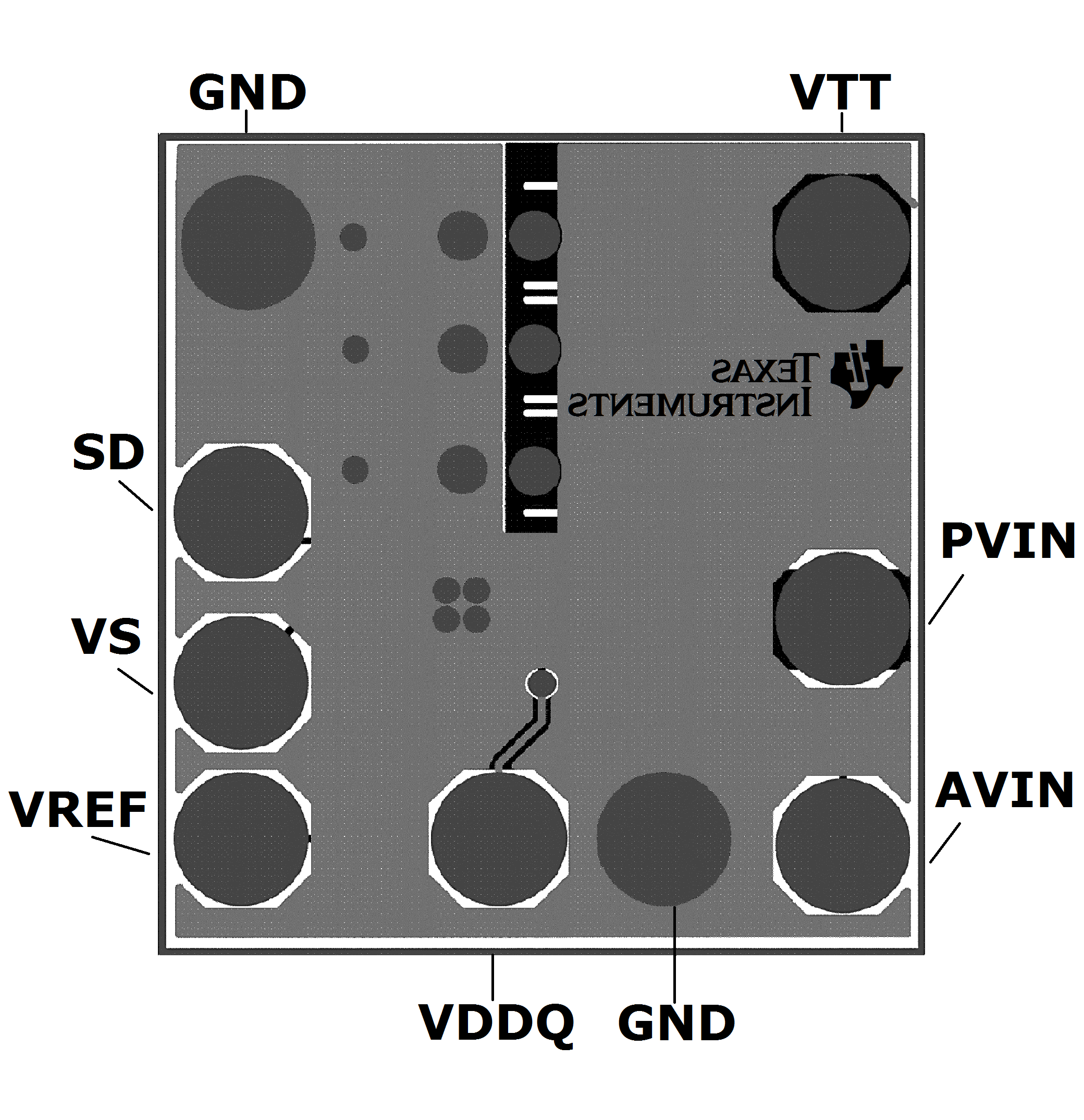
11 Layout
11.1 Layout Guidelines
- The input capacitor for the power rail should be placed as close as possible to the PVIN pin.
- VSENSE should be connected to the VTT termination bus at the point where regulation is required. For motherboard applications an ideal location would be at the center of the termination bus.
- VDDQ can be connected remotely to the VDDQ rail input at either the DIMM or the Chipset. This provides the most accurate point for creating the reference voltage.
- For improved thermal performance excessive top side copper should be used to dissipate heat from the package. Numerous vias from the ground connection to the internal ground plane will help. Additionally these can be located underneath the package if manufacturing standards permit.
- Care should be taken when routing the VSENSE trace to avoid noise pickup from switching I/O signals. A 0.1 µF ceramic capacitor located close to the SENSE can also be used to filter any unwanted high frequency signal. This can be an issue especially if long SENSE traces are used.
- VREF should be bypassed with a 0.01 µF or 0.1 µF ceramic capacitor for improved performance. This capacitor should be located as close as possible to the VREF pin.