SNVSBF5C July 2019 – May 2020 LP3470A
PRODUCTION DATA.
- 1 Features
- 2 Applications
- 3 Description
- 4 Revision History
- 5 Device Comparison Table
- 6 Pin Configuration and Functions
- 7 Specifications
- 8 Detailed Description
- 9 Application and Implementation
- 10Power Supply Recommendations
- 11Layout
- 12Device and Documentation Support
- 13Mechanical, Packaging, and Orderable Information
Package Options
Mechanical Data (Package|Pins)
- DBV|5
Thermal pad, mechanical data (Package|Pins)
Orderable Information
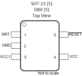
6 Pin Configuration and Functions
DBV Package
5-Pin SOT-23
Top View

Pin Functions
| PIN | I/O | DESCRIPTION | |
|---|---|---|---|
| NO. | NAME | ||
| 1 | SRT | I | Set reset time-out. Connect a capacitor between this pin and ground to select the reset time-out period (tD). tD = 619 × C1 (CSRT in µF and tD in ms). If no capacitor is connected, leave this pin floating. |
| 2 | GND | — | Ground pin. |
| 3 | VCC1 | I | Can be connected to VCC or left floating. DO NOT CONNECT TO GND. |
| 4 | VCC | I | Supply voltage, and reset threshold monitor input. |
| 5 | RESET | O | Open-drain, active-low reset output. Connect to an external pullup resistor. RESET changes from high to low whenever the monitored voltage (VCC) drops below the reset threshold voltage (VIT-). Once VCC exceeds the reset threshold (VIT-) + hysteresis (VHYS), RESET remains low for the reset time-out period (tD) and then deasserts to logic high. |