SNVSBF5C July 2019 – May 2020 LP3470A
PRODUCTION DATA.
- 1 Features
- 2 Applications
- 3 Description
- 4 Revision History
- 5 Device Comparison Table
- 6 Pin Configuration and Functions
- 7 Specifications
- 8 Detailed Description
- 9 Application and Implementation
- 10Power Supply Recommendations
- 11Layout
- 12Device and Documentation Support
- 13Mechanical, Packaging, and Orderable Information
Package Options
Mechanical Data (Package|Pins)
- DBV|5
Thermal pad, mechanical data (Package|Pins)
Orderable Information
7.7 Typical Characteristics
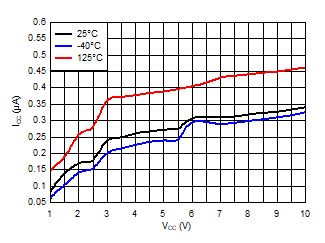
Typical characteristics show the typical performance of the LP3470A device. Test conditions are at TA = TJ = 25°C (unless otherwise noted). Figure 1. Supply Current vs Supply Voltage
  Figure 3. Low Level Output Voltage vs Supply Voltage
  Figure 5. Positive-going Input Threshold VIT+ Accuracy vs Temperature
  Figure 7. Reset Time Delay vs Small Capacitor Values
  Figure 2. Output Voltage vs Supply Voltage for LP3470A293
  Figure 4. Negative-going Input Threshold VIT- Accuracy vs Temperature
  Figure 6. SRT Pin Internal Resistance Overtemperature
  Figure 8. Reset Time Delay vs Large Capacitor Values